Audio Pre-Amplifier Circuit Diagram

This is the Simple Audio Pre-Amplifier Circuit Diagram This simple circuit provides good gain to too audio singnals . Use it in main of an RF oscillators to make an RF transmitter that is very sensitive to sound


Audio Pre-Amplifier Circuit Diagram

Audio Pre-Amplifier Circuit Diagram
Read More

Sensitive Audio Power Meter Circuit Diagram

As a follow-up to the simple audio power  meter described in [1], the author has developed a more sensitive version. In practice,  you  rarely  use  more  than  1 watt  of  audio  power in a normal living-room environment.  The only time most people use more is at a  party when they want to show how loud their  stereo system is, in which case peaks of more  than 10 W are not uncommon. With this circuit, the dual LED starts to light up  green at around 0.1 watt into 8 ohms (0.2 watt  into 4 ohms). Naturally, this depends on the  specific type of LED that is used.

  Sensitive Audio Power Meter Circuit Diagram
Sensitive Audio Power Meter-Circuit-Diagram
Sensitive Audio Power Meter Circuit Diagram
 
Here it is  essential to use a low current type. The capacitor is first charged via D1 and then discharged via the green LED. This voltage-doubler effect  increases the sensitivity of the circuit. Above a level of 1 watt, the transistor limits the current through the green LED and the red LED con ducts enough to produce an orange hue.The red colour predominates above 5 watts. Of course, you can also use two separate ‘normal’ LEDs. However, this arrangement cannot generate an orange hue. For any testing that may be necessary, you should use  generator with a DC-coupled output. If there is a capacitor in the output path, it can cause misleading results.

Reference: Simple Audio Power Meter, Elektor July & August 2008.


Author : Michiel Ter Burg - Copyright : Elektor Electronic
Read More

Audio Amplifiers Using LM386 and NE5534

Many electronic projects require the use of a small audio amplifier. Be it a radio transceiver, a digital voice recorder, or an intercom, they all call for an audio amp that is small, cheap, and has enough power to provide adequate loudness to fill a room, without pretending to serve a disco! About one Watt RMS seems to be a convenient size, and this is also about the highest power that a simple amplifier fed from 12V can put into an 8 Ohm speaker. A very low saturation amplifier may go as high up as 2 Watt, but any higher power requires the use of a higher voltage power supply, lower speaker impedance, a bridge circuit, or a combination of those.

During my many years building electronic things I have needed small audio amps many times, and have pretty much standardized on a few IC solutions, first and and foremost the LM386, which is small, cheap, and very easy to use. But it does not produce high quality audio... For many applications, the advantages weigh more than the distortion and noise of this chip, so that I used it anyway. In other cases I used different chips, which perform better but need more complex circuits. Often these chips were no longer available the next time I needed a small amplifier.

When I last upgraded my computer, I replaced the old and trusty Soundblaster AWE 32 by a Soundblaster Audigy. The new card is better in many regards, but while the old one had an internal audio power amplifier, the new one doesn't! That's bad news, because I have some pretty decent speakers for the PC, which are fully passive. So, I built a little stereo amp using two LM386 chips and installed it inside the computer, fed by the 12V available internally.

But then I wasn't satisfied. The LM386 might be suitable for "communication quality" audio, which is roughly the fidelity you get over a telephone, but for music it's pretty poor! The distortion was awful. So, the day came when I decided to play a little more scientifically with small audio amps, looking for a way to get good performance with simple and inexpensive means.

I set up a test bench with a sine wave oscillator running at 1 kHz, an 8 Ohm speaker, 12V power supply, and the computer with the soundcard and Fast Fourier Transform software. One channel was connected to the oscillator together with the amplifier input, the other channel to the output and speaker. With this setup I measured the harmonic content of the audio signals. I did the tests at an output level of 0.1W, which is typical for moderately loud sound from a reasonably efficient speaker. Also, I used a music signal from a CD player to test the actual sound of each amplifier.

Circuit Project: Small Audio Amplifiers Using LM386 and NE5534

As already said above, the main attraction of the LM386 is the extreme simplicity of its application circuit. You can even eliminate R1 if the signal source is DC-grounded. If the speaker leads are long, you should add an RC snubber across the output to aid stability. Additionally, if you need higher gain (not necessary if the input is at line level), you can connect a 10uF capacitor between pins 1 and 8. That's about all there is to it.

Now the bad news: This circuit produced a very high level of distortion! The second harmonic measured just -28dB from the main output. The third harmonic was at -35dB, while the noise level was at -82dB. There were assorted high harmonics at roughly -45dB. With music, the distortion was really disturbing, and also the noise level was uncomfortably high. The power supply rejection is poor, so that some hum and other supply noise gets through. In short, this was a lousy performance!

Since I had used so many LM386s in my projects, I had several different variations. In my material box I found a slightly newer LM386N-1. So I plugged it into my test amplifier. It was even worse! The second harmonic was at -24dB, the third harmonic at -31dB, while the noise was a tad better at -84dB. Folks, that's a total harmonic distortion of almost 7%! And the 0.1W output level at which this was measured is where such a circuit is about at its best...  The distortion can be plainly seen on the oscilloscope, and a visibly distorted waveform is about the most offending thing an audio designer can ever see!

Looking through my projects, I found one where I had used a GL386 chip. This is just a 386 made by another company. I unsoldered it and put it in my test amplifier. Surprise! It was dramatically better, with the second harmonic at -45dB, and the third at -57dB! The noise floor was -84dB, just like the LM386N-1. But even this level of distortion was plainly audible when listening to music. That's roughly 0.6% THD. Some folks may consider it acceptable for music. I don't, but for communication equipment it's fine. At this point, I decided to see if I could build a better amplifier, that doesn't become too complex nor expensive.

Circuit Project: Small Audio Amplifiers Using LM386 and NE5534

This was the first attempt. A low distortion, fast slew rate, but easy to find and rather inexpensive operational amplifier, driving a simple source follower made of two small transistors. These transistors are not biased, so they work at zero quiescent current, in full class B. The only mechanism that works against crossover distortion here is the high slew rate of the OpAmp, which is able to make the distortion bursts during crossover very short. To say the truth, I didn't expect to get usable performance from this circuit, and was really surprised when it worked much better than the 386! The second harmonic was at -77dB, the third at -79dB!

Also there were many high harmonics at roughly -84dB. That means a THD of about 0.015%.  The noise floor was down at the -120dB level! The power supply rejection was excellent, with no detectable feedtrough. Playing music, this amplifier sounded really good: No audible noise, and the distortion could be heard when paying attention to it, but I doubt that the average person would detect it! Not bad, for a bias-less design!

Just to see how important the slew rate of the OpAmp is, I pulled out the NE5534 and replaced it by a humble 741, which is many times slower. The result was dramatic: The second harmonic still good at -70dB, but the third harmonic was much worse, at -48dB. Also there were many high harmonics at the same -48dB level. Given that second harmonic distortion doesn't sound bad to most people, but third harmonic does, and high harmonics are even worse, it came as no surprise that the amplifier with the 741 sounded bad.

At low volume it sounded particularly bad! So I returned to the oscillator and measurement setup, testing at lower output power, and found that while the second and third harmonics followed the output, the high harmonics stayed mostly constant! So, at very low output, the high harmonics became very strong relative to the output. All this is the effect of the slower slew rate of the 741, which makes it less effective correcting the crossover distortion of the unbiased transistors. Interestingly, the noise floor of the 741 circuit wasn't bad: -118dB.

Just for fun, I tried this circuit with a third OpAmp: The TL071, which is good, but not as good as the 5534. The results: Second harmonic at -72dB, third and the high ones at -60dB, and the noise at -120dB. It's interesting that the second harmonic is much more suppressed than the third one. That must be a balancing effect of the symmetric output stage, and the better symmetry in the TL071 compared to other OpAmps.

It's worthwhile to note that this amplifier can be simplified a lot by using a split power supply. R1, R2, C1, C2 and C4 would be eliminated! But then you need the capacitor removed from C4 to bypass the negative supply line. The positive input of the chip goes to ground, while pin 4 and the collector of Q2 go to the negative supply. The rest stays the same. If you use a +-15V supply, the available RMS output power grows to over 10 Watt! Of course, you then need larger transistors. And since larger transistors are slower, the distortion will rise somewhat. An added benefit of a split supply is that the popping noise when switching on and off is eliminated.

Circuit Project: Small Audio Amplifiers Using LM386 and NE5534

As the next experiment, I decided to get rid of the crossover distortion. For this purpose, I added a traditional adjustable bias circuit with a transistor and a trimpot. Now I also had to add a current source, because with the bias circuit there is no single point into which the OpAmp could put its drive current into both bases! I adjusted the bias for the best distortion, and this was really  a good one! The second harmonic was down right where the test oscillator delivered it, about -80dB, so I couldn't really measure it!

The third harmonic was at -84dB, and the best improvement was that the higher harmonics had simply disappeared! They were all below the noise floor, which stayed at -120dB. Actually, this noise floor seems to come from the soundcard A/D converter, so that the actual noise of this and the above amplifier may even be better! With music, this amplifier sounded perfect - clean and smooth. And I'm pretty confident that the THD is well below the limits of my measurement setup, which is 0.01%.

The quiescent current was around 10mA. When lowering it to about 3mA, the high harmonics started to rise out of the noise floor. If you want to adjust the bias for the exact best quiescent current, there is a simple trick: Lift R4 from the output, and connect it to pin 6. Now the output stage has been left outside the feedback loop, and all its distortion will show up at the output. Watching the signal on an oscilloscope, or even better on a real time spectrum analyzer (soundcard and software), adjust the trimpot to the lowest distortion level.

Have a current meter in the supply line and make sure that you don't exceed 30mA or so of quiescent current, in order to keep the small transistors cool. But most likely the best distortion will be at a current lower than that. Once the adjustment is complete, return R4 to its normal position. Now the full gain and slew rate of the operational amplifier is used to correct the small remaining cross-over distortion of the output stage, and the distortion will certainly disappear from the scope screen, from your ears, and possibly fall below the detection level of the spectrum analyzer!

This circuit can also be run from a split power supply, by exactly the same mods as for the previous circuit. And since the transistors are properly biased, there isn't any significant distortion increase when using larger transistors. Be sure to use some that have enough gain - you have only a few mA of driving available, and with a +-15V power supply and an 8 Ohm speaker, there can be almost 2A of output current! So, you need a gain of 300 at least. There are power transistors in the 4A class that provide such gain, and these are good candidates. The other option is using Darlington transistors, which far exceed the gain needed here. But they will again increase the distortion, not very much, but perhaps enough to make it audible again.
Source: Humo Luden
Read More

10 to 14W Class A Audio Amplifier Circuit Diagram

This is the simple 10 to 14W Class A Audio Amplifier Circuit Diagram. I have built this amplifier and it does sound good. It requires a preamp as it hasn't got much gain. It requires big heat sinks and a large transformer and a great power supply and careful wiring, but in the end it is xtremely simple and it sounds very good. The zener diode rejects any ripple coming from the power supply, But you still only want a ripple of 10mV max. The ripple reaching the input is amplified, so the zener diode gets rid of that, but whatever ripple there is will still reach the power stage.

 10 to 14W Class A Audio Amplifier Circuit Diagram

10 to 14W Class A Audio Amplifier
Read More

Stereo VU Meter Circuit Diagram

This is the simple Stereo VU Meter Circuit Diagram. This project will indicate the volume level of the audio going to your speakers by lighting up LEDS. The LEDS can be any color so mix them up and really make it look good. The input of the circuit is connected to the speaker output of your audio amplifier. You want to build two identical units to indicate both right and left channels. The input signal level is adjusted by the 10k ohm VR. If you wish to make a very large scale model of this unit and hang it on your wall there is an optional output transistor that can drive many LEDS at once. The unit I built drove three LEDS for each output. The sequence of the LEDS lighting are as follows Pin 1, 18, 17, 16, 15, 14, 13, 12, 11, 10.

Stereo VU Meter Circuit Diagram


Stereo VU Meter Circuit Diagram
Read More

Equalising HEXFETs Circuit Diagram

When experimenting with audio output stages featuring multiple HEXFETs it quickly becomes apparent that the total power is not divided equally among the individual transistors. The reason for this lies in the wide part-to-part variations in gate-source voltage, which in the case of the IRFP240 (or IRFP9240) can be from 2 V to 4 V. Source resistors in the region of 0.22 Ω as commonly seen in amplifier circuits (see example circuit extract) help to counteract this, but usually not to a sufficient extent. One possible solution to this problem is to ‘select’ the transistors used so that their gate-source voltages match as closely as possible.

 Equalising HEXFETs Circuit Diagram


For building prototypes or very short production runs this is feasible, but requires additional manual effort in testing the components, and, of course, more transistors must be ordered than will finally be used. The circuit idea shown here allows differences in gate-source voltage between pairs of transistors to be compensated for by the addition of trimmer potentiometers: the idea has been tested in simulation using Simetrix. The second circuit extract shows the required changes.
Read More

Voice Scrambler Circuit Diagram

With this circuit you can modify how your voice sounds by changing the pitch of your voice. This circuit can be connected to a phone and with a duplicate circuit on the end of the phone line, you can have a scrambled voice communication. The way the circuit works is as follows: If we cut the circuit in half at the T2 transformer and include the LM324 on the left side, you will see that the LM324 portion of the circuit is a tone oscillator which shifts the frequency of all input signals to a new higher frequency. When the voice and the tone oscillator mix frequencies the voice is not recognized. The voice signal is then inputted to the second stage which again shifts the voice signal again. I recommend that the first stage be tuned to a frequency that is 100hz lower then the second stage.

 Voice Scrambler Circuit Diagram


Read More

Surf Sound Synthesizer Circuit Diagram

Many people who live close to the ocean have the benefit of being lulled to sleep by the sound of the surf. This circuit may provide a similar benefit to all those poor unfortunates who don’t live near the seaside but who do have the small consolation that they don’t have to worry about rust and corrosion in a salty atmosphere. The circuit consists of four unsynchronised oscillators which are mixed together to modulate a white noise source to simulate the more or less random nature of surf sounds. You won’t hear the waves crashing but the ebb and flow of the white noise will help mask other noises which would otherwise disturb your sleep.


Surf Sound Synthesizer circuit diagram


The four oscillators are based on four op amps in a TL074 or TL084 quad op amp package (IC1). IC1a, IC1b, IC1c & IC1d are configured as Schmitt trigger oscillators with their operating frequencies defined by the resistor connected between their outputs (pins 1, 7, 8 & 14) and the respective inverting inputs (pins 2, 6, 9 & 13), as well as the electrolytic capacitors connected between these latter pins and 0V. The result is a triangle waveform at each of the respective inverting inputs and square waves at the same frequencies at the op amp outputs. We don’t use the square outputs but instead feed the four triangle waveforms to op amp IC2a which is connected as a mixer. Its output is used to drive and modulate a noise source based on NPN transistor Q1. This is operated with reverse bias across its base-emitter junction and the controlled reverse current is very noisy.

By varying the amount of reverse bias, we vary the amount of white noise produced. Since the amount of noise produced by the transistor varies markedly between types, the gain of IC2a can be varied over a wide range to produce the optimum output voltage to drive Q1. From there, the noise signal from the emitter of Q1 is fed via a 47nF capacitor to op amp IC2b which can also have its gain varied over a wide range to drive IC3, an LM386 power amplifier which drives the loudspeaker. In use, first adjust trimpot VR2 to set the volume level from the loudspeaker, then adjust trimpot VR1 to get the best range of white noise which simulates the surf sounds. Sleep well.
Read More

External Winamp Control Circuit Diagram

Nowadays, winamp have full support to keyboard shortcuts. But some time ago, when Winamp didn’t have this feature, I was thinking in a way I could change the music just by pressing one button, it would make things faster and easier to change songs, specially during games. So I decided to make a external control to it. I found one winamp plugin that shows how to configure a external control using the Serial Port, being able to make 4 or 15 buttons control. I decided to make this, step-by-step, how to do it, hope you enjoy.


Material:
  • 4 push-buttons
  • SERIAL connector
  • Connector Box
  • Cable


Necessary tools:
  • Soldering iron and accessories
You can put the buttons wherever you want, I decided to put mine in one old diskbox.
I decided to use a network cable to connect the Serial connector to the buttons, because its easier to organize and makes the work simplier and faster.

The scheme:

Making the control:
  • Looking in the scheme, we see that we have to connect one side of each buttons to one cable, these will be solded in the pin number 4.


  • After have done the soldering in one side of each button, you must then connect the other side with a cable that goes to the pins of the serial, now however is important that they are connected with the indicated pins (Just follow the scheme) .
    Here you can see a picture of my work until now, it looks quite ugly I know, sorry.


Configuring the Software
    The software I used in this was COM-port Winamp Control V.1.42.
  • You must set the COM port you are using, usually normal computers have up to 2 ports, so just select the one you plugged the control.
  • Select the number of buttons your control have. (In this HowTo, we’d choose the “4 buttons”)
  • Now you must remap the buttons, its now the time when you’ll see if everything is working. If you are able to remap all the buttons, congrats, its working!!
  • Its ready, now the last step, you have to configurate what you want the buttons to do. This can be found in the “WINAMP” of the program. There you can setup many different options, like Volume Up, Volume Down, Next Song, Previous Song.
  • One cool stuff is there in “Type:”, where you can configure the way you wanna the buttons pressing to respond.
  • Click: Just one click to make it work. Can work with one or double-click.
  • Down/Up: This will activate the option when you press and a different one when you release the buton.
  • Turbo: Here you can configure the options for holding the button, usually used for Volume Up and Down.
  • Clicks + Turbo: You can configure “Clicks” and “Turbo”Option at the same time
  • Clicks + Hold: You can configure “Clicks” and “Hold” Option at the same time
In the end, I put the buttons in that disk case I told before, and this are the results:


I don’t know if I was clear enought in this HowTo, I will re-check this sometime.
If you liked this, have any correction or advice, please leave a comment! 
Source : link
Read More

5.8 Watt Audio Power Amplifier Circuit Diagram

This circuit use TA7222AP to amplifiers audio signal .The price only $0.99 and can provide 5.8 watt with Muting Control.Power supply can use for 8-12Vdc it is a good idea to use for car audio power amp , coin-op machine game, security system etc. link


Fig 1. TA7222AP pin out


Pin Name Description
1 Vcc Supply Voltage
2 RR Ripple Reject
3 MC Muting control
4 OP AF Signal Input
5 FB FB Filter
6 GA Gain adjust
7 GND Ground
8 GND Ground
9 OP AF Output
10 BS BootStrap


Fig 2. schematic for 5.8 watt audio power amplifier
Read More

CD Player Adapter For Car Circuit Diagram

Whenever I'm in the car listening to my favourite CD, it always happens; my batteries go dead. To solve that problem, I built this extremely simple regulator circuit. It steps down the 12V from the lighter socket to 9V which is used by the CD player. Different CD players (I have a Sony Discman) may require different voltages, so just use the correct regulator. All the 78xx series regulators have the same pin out, so the circuit is universal.

CD Player Adapter For Car Circuit Diagram


CD Player Adapter For Car Circuit Diagram


Part           Total Qty.                     Description

C1                      1                        1000uF 25V Electrolytic Capacitor   
C2                      1                        10uF 25V Electrolytic Capacitor   
C3                      1                        1uF 15V Elextrolytic Capacitor   
C4                      1                        0.1uF 15V Electrolytic Capacitor   
U1                      1                        7809 Or Other Regulator (See "Notes")    See Notes
MISC                  1                      Cigarette Lighter Plug, Plug For CD Player (See "Notes"),      Heat Sink For U1, Wire, Case.   
   
Notes
  • The voltage your CD player needs will determine which regulator you use. For 9V, use the 7809. For 6V, use the 7806. For the unlikely 5V use the 7805. Remember that whatever regulator you use, you will need to heat sink it. The metal case or metal cover on the case makes a great heat sink.
  • I built the circuit in a small case with the long wire to the cigarette lighter plug coming out one end, then another, slightly shorter wire going out the other end to the CD player.
  • Triple check your wiring. You would hate to ruin an expensive CD player because you reversed one of the connections or hooked the regulator up backwards. Link
Read More

Simple Tremolo Effect Circuit Diagram

This tremolo effect circuit uses the XR2206 and the TCA730 IC which is designed as an electronic balance and volume regulator with frequency correction. The circuit is use full for stereo channels and it also has the ability to simulate the Lesley effect aka rotating loudspeaker effect.

 How does the tremolo effect circuit works
Balance and volume settings are done with a linear potentiometer for both channels. If this potentiometer is replaced with an AC voltage source, a periodic modulation of the input signal can be achieved. This AC voltage source comes from the function generator IC XR2206. This IC generates square, triangle and sine wave signals but for this project we use only the sine wave.

IC Tremolo effect circuit schematic

Circuit Project: DIY Tremolo Effect Circuit

The modulation voltage can be varied with P1 from 1 Hz up to 25 Hz. Resistor R3 sets the operation level of the sine wave generator. R5 and R6 set the DC voltage and the sine wave amplitude at the output. C2 is a ripple filter. The square wave output of the XR2206 drives T2 and a LED to optically display the frequency.

The modulating voltage reaches pin 13 of TCA730 via P3 and R10. This input functions as the volume control or in this case the volume modulation. The degree of the balance modulation (Lesley effect) can be varied with P2. A regulated power supply using 7815 IC is recommended. Do not use a non-stabilized power supply since the current variations would influence the modulation negatively.
Attach the 7815 IC to a good heat sink (about 10 cm2).
Read More

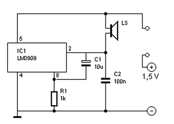
Audio Lm 3909 IC-conduction tester Circuit Diagram

This tiny conductivity tester works with LM 3909. The tester makes a beeping sound if the resistance between the test probes between 0 and 100 O lies. Due to the volume of the beep, the resistance between the test probes can be determined.

Audio Lm 3909 IC-conduction tester Circuit Diagram

Audio Lm 3909 IC-conduction tester Circuit Diagram
Parts List

     R1 = 1 k
     C1 = 10 uF
     C2 = 100 nF
     LS = Loudspeaker 12 to 16 Ω
     IC1 = LM 3909
Read More

Digital Volume Control Circuit Diagram

This digital volume control has no pot to wear out and introduces almost no noise in the circuit. Instead, the volume is controlled by pressing UP and DOWN buttons. This simple circuit would be a great touch to any home audio project.

Schematic

Schematic for amp

Parts:


Part

Total Qty.

Description
C1
1
0.1uf Ceramic Disc Capacitor
U1
1
DS1669 Digital Pot IC (See Notes)
S1, S2
2
Momentary Push Button Switch
MISC
1
Board, Wire, Socket For U1

Notes:

1. U1 is available from Dallas Semiconductor.
2. S1 turns the volume up, S2 turns it down.
3. The input signal should not fall below -0.2 volts.
4. Using a dual polariity power supply (+-5V works fine) will cure most clipping problems. You will have to check the data sheet for the correct pins to connect your voltages. Link
Read More

Bells Ring Generator Circuit Schematic

This circuit generates a dual-tone bells ringing similar to most door-bell units. It can be used in many applications other than door-bell. In the Notes below several options will be given in order to suit different needs. The circuit as shown in the diagram generates a "Ding-tone" when P1 is pressed and a "Dong-tone" when P1 is released. IC1D is the first-tone frequency generator and IC1F generates the second-tone.

Q2, Q5 and related components act as shape and decay controls of the two tones, trying to imitate as close as possible the bells sound. Their outputs are mixed (R7 & R13), filtered (C5) and boosted by a simple class-A audio amplifier (Q3 & Q4) in order to drive the loudspeaker. The amplifier is switched-on by Q1 when P1 is pressed, then is switched-off some seconds after P1 is released: this time-delay is fixed by C1 & R2. In this way the circuit will draw a negligible current when in stand-by mode.

Circuit diagram:
 bells ring generator schematic circuit diagram
Bells Ring Generator Schematic Circuit Diagram


Parts:

R1,R3,R7,R9,R13_10K 1/4W Resistors
R2_______________1M5 1/4W Resistor
R4______________27K 1/4W Resistor
R5,R11__________47K 1/4W Resistors
R6,R12_________220K 1/4W Resistors
R8_______________2M2 1/4W Resistor
R10_____________33K 1/4W Resistor
C1_______________2µ2 25V Electrolytic Capacitor
C2______________47µF 25V Electrolytic Capacitor
C3,C8___________10µF 25V Electrolytic Capacitors
C4,C7___________10nF 63V Polyester Capacitors
C5,C6__________100nF 63V Polyester Capacitors
C9_______________4µ7 25V Electrolytic Capacitor
C10______________1µF 25V Electrolytic Capacitor
D1-D5_________1N4148 75V 150mA Diodes
IC1__________MC14106 or 40106 Hex Schmitt Inverter IC
Q1_____________BC337 45V 800mA NPN Transistor
Q2,Q3,Q5_______BC238 25V 100mA NPN Transistors
Q4 ____________BC327 45V 800mA PNP Transistor
PH______________Photo resistor (any type) (see Notes)
P1______________SPST Pushbutton (see Notes)
SW1_____________SPST Switch
SPKR____________8 Ohm Loudspeaker
B1______________3V Battery (two 1.5V AA or AAA cells in series etc.)
Parts added to optional modification:
R14____________220K 1/4W Resistor
R15______________1M 1/4W Resistor

Notes:
  • To obtain a "Ding-Dong" operation when pushing on P1, no matter when it is released, you must modify the circuit as shown in the frame placed at the low-right corner of the circuit diagram. D4 must be removed. C10 & R15 set the time-delay separating first and second tone.
  • To obtain a one-tone-only generator, wire the circuit as in the optional modification, making the following changes:
  • C9 = 100nF 63V Polyester Capacitor.
  • Omit R9 to R13 & R15; C7, C8 & C10; D2, D4, D5 & Q5.
  • Connect to negative supply pins 11 & 13 of IC1 and left open pins 10 & 12.
  • An amusing application of this circuit wired as in the original schematic, is to use a photo-resistor in place of P1, then placing the unit near the flashing lamps of your Christmas tree. A soft bell sound may be heard at switch-on and switch-off of the lamp chosen.
  • To obtain higher output power you may substitute R8, Q3 & Q4 with an audio amplifier IC like the LM386 or LM380. In this case power supply must be raised to 6 - 12V but at the same time R4 & R10 should be changed to adjust bell-tone frequencies.
  • Good tone frequencies are roughly 2000 and 1650Hz respectively.
  • When in stand-by mode, current drawing of the circuit is 200µA @ 3V supply: therefore SW1 can be omitted.
Source: Red Free Circuit Design
Read More

Melody Generator Circuit Diagram

Here is the simplest melody generator circuit you can make using an IC.The UM66 series are CMOS IC’s designed for using in calling bell, phone and toys. It has a built in ROM programmed for playing music. The device has very low power consumption.Thanks for the CMOS technology.The melody will be available at pin3 of UM66 and here it is amplified by using Q1 to drive the speaker.Resistor R1 limits the base current of Q1 within the safe values.Capacitor C1 is meant for noise suppression.


Parts:

R1 = 4.7K
IC = UM66T
Q1 = 2N2222
C1 = 10uF-16v
S1 = On/Off Switch
B1 = 1.5 - 4.5 Battery
SP = 2R Speaker

Notes:
  • Power supply must be between 1.5V & 4.5V .Do not exceed 4.5 V.
  • Speaker can be driven with external NPN transistor.
  • Melody begins from the first note if power is reseted.
  • Assemble the circuit on a good quality common board.

Read More

4 Channel Portable Audio Mixer Circuit Diagram

The target of this project was the design of a small portable mixer supplied by a 9V PP3 battery, keeping high quality performance. The mixer is formed assembling three main modules that can be varied in number and/or disposition to suit everyone needs. The three main modules are:

Input Amplifier Module: a low noise circuit equipped with a variable voltage-gain (10 - 100) preset, primarily intended as high quality microphone input, also suitable for low-level line input.

Tone Control Module: a three-band (Bass, Middle, Treble) tone control circuit providing unity-gain when its controls are set to flat frequency response. It can be inserted after one or more Input Amplifier Modules and/or after the Main Mixer Amplifiers.

Main Mixer Amplifier Module: a stereo circuit incorporating two virtual-earth mixers and showing the connection of one Main Fader and one Pan-Pot.

The image below shows a Block diagram of the entire mixer featuring four Input Amplifier Modules followed by four in-out switchable Tone Control Modules, one stereo Line input, four mono Main Faders, one stereo dual-ganged Main Fader, four Pan-Pots, a stereo Main Mixer Amplifier Module and two further Tone Control Modules switchable in and out for each channel, inserted before the main Left and Right outputs.

Obviously this layout can be rearranged at everyone wish. An astonishing feature of this design lies in the fact that a complete stereo mixer as shown below in the Block diagram draws less than 6mA current!

Block diagram:

4 channel input mixer

Input Amplifier Module
Circuit Diagram:

Parts:

R1 = 22K - 1/4W Resistor
R2 = 22K - 1/4W Resistor
R3 = 47K - 1/4W Resistor
R4 = 47K - 1/4W Resistor
R5 = 47K - 1/4W Resistor
R6 = 4K7 - 1/4W Resistor
R7 = 22K - 1/4W Resistor
R8 = 220R - 1/4W Resistor
R9 = 2K - 1/2W Trimmer Cermet (See Notes)
R10 = 470K - 1/4W Resistor
R11 = 560R - 1/4W Resistor
R12 = 100K - 1/4W Resistor
R13 = 220R - 1/4W Resistor

C1 = 470nF - 63V Polyester Capacitor
C2 = 100µF - 25V Electrolytic Capacitor
C3 = 2µ2 - 63V Electrolytic Capacitor
C4 = 2µ2 - 63V Electrolytic Capacitor
C5 = 2µ2 - 63V Electrolytic Capacitor
C6 = 47pF - 63V Ceramic Capacitor
C7 = 4µ7 - 63V Electrolytic Capacitor
C8 = 100µF - 25V Electrolytic Capacitor
Q1 = BC560C - 45V 100mA Low noise High gain PNP Transistor
Q2 = BC550C - 45V 100mA Low noise High gain NPN Transistor
IC1 = TL061 - Low current BIFET Op-Amp

Circuit Description:

The basic arrangement of this circuit is derived from the old Quad magnetic pick-up cartridge module. The circuit was rearranged to cope with microphone input and a single-rail low voltage supply. This low-noise, fully symmetrical, two-transistor head amplifier layout, allows the use of a normal FET input Op-Amp as the second gain stage, even for very sensitive microphone inputs. The voltage-gain of this amplifier can be varied by means of R9 from 10 to 100, i.e. 20 to 40dB.

Notes:
  • R9 can be a trimmer, a linear potentiometer or a fixed-value resistor at will.
  • When voltage-gain is set to 10, the amplifier can cope with 800mV peak-to-peak maximum Line levels.
  • Current drawing for one Input Amplifier Module is 600µA.
  • Frequency response is 20Hz to 20KHz - 0.5dB.
  • Total Harmonic Distortion measured with voltage-gain set to 100: 2V RMS output = <0.02%>
  • Total Harmonic Distortion measured with voltage-gain set to 10 & 33: 2V RMS output = <0.02%>
  • THD is much lower @ 1V RMS output.
  • Maximum undistorted output voltage: 2.8V RMS.

Read More

Music Generator Using UM66 Circuit Diagram

UM66 is a pleasing music generator IC which works on a supply voltage of 3V. the required 3V supply is given through a zener regulator. its out put is taken from the pin no1 and is given to a push pull amplifier to drive the low impedance loud speaker. A class A amplifier before push pull amplifier can be used to decrees the noise and improve out put. UM66 is a 3 pin IC package just looks like a BC 547 transistor.

Music Generator Using UM66 Circuit Diagram

 A music - melody generator schematic Circuit Diagram using UM66
A Continuous Music Generator Circuit Diagram

Parts:

R1 = 4.7K
C1 = 10uF-25v
D1 = 3.3v Zener
Q1 = SK100
Q2 = SL100
IC = UM66
SP = 8 ohm

Pin out of UM66 IC:
  1. Output----Melody Output
  2. +Vdd-----Positive power supply
  3. -Vss------Negative Power supply

Features of UM66T series:
  • 62 Note ROM Memory
  • Voltage rating: 1.3V to 3.3 V
  • Power on reset
Read More

Cuckoo Sound Generator Circuit Schematic

This circuit generates a two-tone effect very much alike the cuckoo song. It can be used for door-bells or other purposes thanks to a built-in audio amplifier and loudspeaker. Used as a sound effect generator it can be connected to external amplifiers, tape recorders etc. In this case, the built-in audio amplifier and loudspeaker may be omitted and the output taken across C8 and ground. There are two options: free running, when SW1 is left open, and one-shot, when SW1 is closed. In this case a two-tone cuckoo song will be generated at each P1 pressing.

Circuit diagram:

Cuckoo Sound Generator Circuit Schematic

Parts:

R1,R5___________1K 1/4W Resistors
R2_____________50K 1/2W Trimmer Cermet
R3______________8K2 1/4W Resistor
R4_____________82K 1/4W Resistor
R6______________1M 1/4W Resistor
R7,R17,R20,R21_22K 1/4W Resistors
R8,R10,R11,R19_10K 1/4W Resistors
R9____________150K 1/4W Resistor
R12_____________4K7 1/4W Resistor
R13___________100K 1/4W Resistor
R14___________220R 1/4W Resistor
R15,R22________20K 1/2W Trimmers Cermet
R16____________10R 1/4W Resistor
R18___________200K 1/2W Trimmer Cermet
C1,C11_________47nF 63V Polyester or Ceramic Capacitors
C2,C10,C12____220µF 25V Electrolytic Capacitors
C3____________220nF 63V Polyester or Ceramic Capacitor
C4_____________22nF 63V Polyester or Ceramic Capacitor
C5,C6,C8,C9___100nF 63V Polyester or Ceramic Capacitors
C7,C13,C14_____10µF 63V Electrolytic Capacitors
D1,D2,D3,D6__1N4148 75V 150mA Diodes
D4,D5_________BAT46 100V 150mA Schottky-barrier Diodes
Q1,Q2_________BC547 45V 100mA NPN Transistors
IC1____________7555 or TS555CN CMos Timer IC
IC2____________4093 Quad 2 input Schmitt NAND Gate IC
IC3____________4017 Decade counter with 10 decoded outputs IC
IC4___________LM386 Audio power amplifier IC
P1_____________SPST Pushbutton
SW1____________SPST Switch
SPKR___________8 Ohm Loudspeaker

Circuit Dis....
IC1 is wired as a square wave generator and produces both tones of the cuckoo song. The frequency of the higher one (667Hz) is set by means of Trimmer R2. When IC2D output goes low, a further Trimmer (R22) is added to IC1 timing components via D6, and the lower tone (545Hz) is generated. To imitate closely the cuckoo song, the square wave output of IC1 is converted to a quasi-sinusoidal wave form by R3, R4, C3 and C4, then mixed with the white noise generated by Q1, R6.

Q2 has two purposes: it mixes the two incoming signals and gates the resulting tone, shaping its attack and decay behavior by means of the parts wired around its Emitter. IC4 is the audio power amplifier driving the speaker and R15 is the volume control. The various sound and pause timings for the circuit are provided by the clock generator IC2A driving the decade counter IC3. Some output pins of this IC are gated by IC2C, IC2D and related components to drive appropriately the sound generator and the sound gate.

When SW1 is left open the circuit operates in the free-running mode and the cuckoo song is generated continuously. When SW1 is closed, the circuit generates two tones then stops, because a high state appears at the last output pin (#11) of the decade counter IC: therefore the count is inhibited by means of D1 feeding pin #13. The circuit is reset by a positive pulse at pin #15 of IC3 when P1 is pressed.

Setup:

Best results will be obtained if the two tones frequencies are set precisely, i.e. 667Hz for the first tone and 545Hz for the second: in musical terms this interval is called a Minor Third. Obviously a digital frequency counter, if available, would be the best tool to setup R2 and R22, but you can use a musical instrument, e.g. a piano or guitar, tuning-up the notes accurately by ear.
  • Disconnect temporarily R22 from D6 anode.
  • Connect the digital frequency counter to pin 3 of IC1.
  • Adjust R2 in order to read 667Hz on the display.
  • Connect R22 to negative ground and adjust it to read 545Hz on the display.
  • Restore R22 - D6 connection.
Tuning by ear:
  1. Disconnect temporarily R22 from D6 anode.
  2. Disconnect C8 from Q2 Collector and connect it to R4, C4 and C5 junction.
  3. Adjust R2 in order that the tone generated by the loudspeaker is at the same pitch of the reference note generated by your musical instrument. This reference note will be the E written on the stave in the fourth space when using the treble clef.
  4. Connect R22 to negative ground and adjust it in order that the tone generated by the loudspeaker is at the same pitch of the reference note generated by your musical instrument. This second reference note will be the C-sharp written on the stave in the third space when using the treble clef.
  5. Restore R22 - D6 and C8 to Q2 Collector connections.

Notes:
  • The master clock can be adjusted by means of R18.
  • The percentage of hiss and sound in the mixing circuit, setting the tone character, can be varied changing R8 and R7 values respectively.
  • Any kind of dc voltage supply in the 12 - 15V range can be used, but please note that supply voltages below 12V will prevent operation of the white noise generator.
  • An amusing application of this circuit is to use a photo-resistor in place of P1, then placing the unit near the flashing lamps of your Christmas tree. A sweet cuckoo song will be heard each time the lamp chosen will illuminate.
Source: Red Free Circuit Design

Read More

TDA2052 Active Audio System Circuit Diagram

This active audio audio system use three TDA2052 chips and 5 speakers ( one woofer, two tweeters and two midranges ). For this TDA2052 active audio system we need dual 20 volts power supply and five volts supply for the stand by function.To the input of the every audio IC chip is placed an audio filter for filtering the audio signal for used speakers ( low pass for woofer , high pass for midranges and tweeters)

TDA2052 Active Audio System Circuit Diagram


The subwoofer plays the 20 to 300 Hz frequency range, while the remaining 300 Hz to 20KHz are sent to two separate channels with stereo effect.If one of the amplifier is affected by clipping distortion the others amplifiers are not affected .
Read More