Logical Tip with Inverters and Diode

This simple logic tip with inverters is implemented with three NOT (NO) gates, one rectifier diode, two LEDs and two resistors. The tip or logical probe allows to determine the logical state of any point in a digital circuit. The signal is applied to the IN input.

This tip is very easy to construct, because it uses few elements that could easily be located on a very narrow printed circuit board (PCB). Such a plate could be placed without problems in a thick tube or pencil in disuse.

Operation of the logical tip with inverters

If the signal being measured is a "high" logic level:


  1. The upper inverter inverts the signal (logic level "low") and the red LED does not turn on.
  2. The common diode is polarized live. The signal is inverted twice by the two inverters in cascade and the green LED lights up (logic level "high").


If the signal being measured is a "low" logic level:
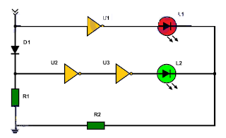

  1. The upper inverter inverts the signal and the red LED turns on (logic level "high").
  2. The common diode does not drive. As a consequence there is a "low" logic level at the anode of the diode. This low level is reversed twice by the inverters in cascade and the green LED does not turn on (logic level "low").
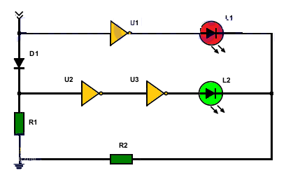
Logical Tip with Inverters and Diode


Resistor R2 limits the current flowing through the LEDs (green and red)

To implement the circuit you need an integrated circuit TTL (Transistor Transistor Logic) SN7404 with 6 NOT gates. Keep in mind that the voltage source that will power this circuit is 5 volts and can only be used to test digital circuits manufactured with TTL integrated circuits.

Take into account that the ground connection (0 volts) of the circuit under test and the 0V terminal of the logic tip must be the same.

Note: There are three integrated NOT gates that are not used in circuit operation. They should put their inputs at 5 volts (logical level "high").

List of tip components / logical shadow
1 TTL integrated circuit SN7404 (6 inverters / NOT gates). Only 3 (U1, U2, U3) are used
1 rectifier diode 1N4001 or similar (D1)
2 common LEDs (red, green) (L1, L2)
1 resistor of 220 ohms, 1/4 watt (R2)
1 resistance of 10K, 1/4 watt (R1)
Read More

Simple 50 watt 12 VDC to 220 VAC Power Inverter

This is the Simple 50 watt 12 VDC to 220 VAC Power Inverter. Power inverter (UPS Uninterruptible power supply) is a very useful device which can convert Low voltage from a DC source to high voltage AC. The most common power inverter is 12V to 240V inverter. Perhaps that is because 12V batteries are common. This type of power inverter usually draws current from a DC battery. This battery should be able to provide a high flow of electric current. 

Normally lead acid batteries can server this purpose well. This current is then converted to 240V square wave alternative current so that we may empower those electric appliances which work on 240V instead of 12V. Inverter falls in the category of expensive devices so many people don’t buy them even they need them. What if I tell you how to build an inverter (UPS Uninterruptible power supply) yourself?

 Iverter circuit diagram
Iverter circuit diagram

Parts.
Transformer 12+12/220 (50W) ( you can make your own inverter transformer visit Make your own homemade (DIY) Electric Transformer)
2, metter copper wire (for winding)
2 Transistors 1047
2 Heat sinks to fit power transistors
Some wiring wire (for connections)
A wiro-board (To build circuit on)
A 12V battery of 12V power supply for testing purposes
1 Resisters 1 k

Method:
First of all you have to make some changes in transformer. If u are using 500 V transformer then take 18 to 22 gauge copper wire and on the one side of transformer’s core make five turn and put a point on it, and turn this point, and again turn the wire five times on the same direction. In this way u get three terminals. If u r connect the transformer to 220 V power supply then it gives 1.5 V on both terminals. Now put transformer D1047 on the palm of your hand and turn it such a way that number appears your way. Now you will see three points. The point on your left side is known as (B) Base, middle one is E and the right one is collector(C). (These are the information only for D1047)

connect the E of both sides of transistors with the outer terminal of secondary coil, after that connect the both outer terminals of the third coil with the base of the both heat sinks of transistor. then connect the collectors of both side by wires n then connect the 500 ohm resistor on emitter and resistor on either side. Now connect the middle terminal of primary coil by one to two ft long wire and clip (crocodile) it and attach this terminal always by the positive terminal, and with the negative terminal of battery connect the both collectors of transistor.

After that the central point of the third coil and a wire attach it with emitter to connect using a heavy ampere switch between both terminals of the Inverter primary coil to apply a capacitor which will prevent the current from the sparking. inverter will switch on as soon as starting to work.

Working:
With both the terminals of battery connect the positive and negative wires to its terminals positive to positive and negative to negative and then open the switch, slightly vibration starts in the inverter as switch is open. Now you can run it into 1 to 500 watt load.
This inverter also can charge the batteries, you just need to( on and off) the switch.

Charging:
You will need to switch off for battery charging and connect the primary coil indirectly with 220 V of power supply, after that battery will start charging. To converts it into UPS you needs only one relay. These relays are AC 220 V and 4.4 terminals.
For online help visitPak Science and technology Forum

Inverter circuit diagram for battery charging :

Inverter circuit diagram for Inverter operation :
Power Inverter Wattage Chart
inverters Transformer voltages (Input)
Transformer Amps Transformer watt No of Transistors D1047
50 watt inverter 12 V 4 A 50 W 2
100 watt inverter 12 V 10 A 100 W 4 to 6
300 watt inverter 12 V 25 A 300 W 6 to 8
500 watt inverter 12 V 40 A 500 W 8 to 10
1000 watt inverter 24 V 45 A 1000 W 20 to 26
3000 watt inverter 24 V 125 A 3000 W 40 to 50
5000 watt inverter 48 V 105 A 5000 W 60 to 70
Note. table shows that requirement of D1047 transistors for different power inverter wattage
Read More

Ups System mini Circuit Diagram

This is the Ups System mini Circuit Diagram. This Ups System mini circuit provides an uninterrupted  power supply (UPS) to operate 12V, 9V and 5V DC-powered instruments at up to 1A current. The backup battery takes up the load without spikes or delay when the mains power gets interrupted. It can also be used as a workbench power supply that provides 12V, 9V and 5V operating voltages. The circuit immediately disconnects the load when the battery voltage reduces to 10.5V to  prevent deep discharge of the battery.  LED1  indication  is  provided  to  show  the full charge voltage level of the battery. miniature white LEDs (LED2 and  LED3) are used as emergency lamps during power failure at night. 


Mini Ups System Circuit Diagram

A standard step-down transformer provides 12V of AC, which is rectified by diodes D1 and D2. Capacitor C1 provides ripple-free DC to  charge the battery and to the remaining circuit. When the mains power is  on, diode D3 gets forward biased to charge the battery. Resistor R1 limits the charging current. Potentiometer VR1 (10k) with transistor T1 acts as the voltage comparator to indicate the voltage level. VR1 is so adjusted that LED1 is in the ‘off’ mode. When the battery is fully charged, LED1 glows indicating a full voltage level of 12V. 

When the mains power fails, diode D3 gets reverse biased and D4 gets forward biased so that the battery can automatically take up the load without any delay. When the battery voltage or  input voltage  alls below 10.5V, a cut-off circuit is used  to prevent deep discharging of the battery. Resistor R3, zener diode  ZD1 (10.5V) and transistor  T2  form  the  cut-off circuit. When the voltage level is above 10.5V, transistor T2 conducts and its base becomes negative (as set by R3, VR2 and ZD1). But when the voltage reduces below  10.5V, the zener diode stops conduction and the base voltage of transistor T2 becomes positive. It goes into the ‘cut-off’ mode and prevents the current in the output stage. Preset VR2 (22k) adjusts the voltage below 0.6V to make T2 work if the voltage is above 10.5V. 

When power from the mains is available, all output voltages—12V, 9V and 5V—are ready to run the load. On the other hand, when the mains  power is down, output  volt-ages can run the load only when the  battery is fully charged (as indicated by LED1). For the partially charged battery, only 9V and 5V are available. Also, no output is available when the voltage goes below 10.5V. If battery voltage varies between 10.5V and  13V, output at terminal A may also vary between 10.5V and 12V, when the UPS system is in battery mode.
Outputs at points B and C provide 9V and 5V, respectively, through regulator ICs (IC1 and IC2), while output A provides 12V through the zener diode. The emergency lamp uses two ultra-bright white LEDs (LED2 and LED3) with current limiting resistors R5 and R6. The lamp can be manually switched ‘on’ and ‘off’ by S1. The circuit is assembled on a general purpose PCB. There is adequate space between the components to avoid overlapping. heat sinks for transistor T2 and regulator ICs (7809 and 7805) to dissipate heat are used. 

The positive and negative rails should be strong enough to handle high current. Before connecting the circuit to the battery and transformer, connect it to a variable power supply. Provide 12V DC and adjust VR1 till LED1  glows. After setting the high voltage  level, reduce the voltage to 10.5V and adjust  VR2  till  the  output  trips  off.  After  the  settings  are complete, remove the variable power sup-ply and connect a fully-charged battery to the terminals and see that LED1 is  on. After making all the adjustment connect the circuit to the battery and transformer. The battery used in the circuit is a 12V, 4.5Ah UPS battery. 
Read More

Mini Power Inverter Circuit Diagram

Simple Mini Power Inverter Circuit Diagram. Even robot systems occasionally need a negative supply voltage for some purpose or other, and in this kind of application in particular there is a need for an effective circuit that does  not  make  greater demands  then  necessary in terms of current or space. If a low current 5 V supply is needed and only +5 V is available, a natural manufacturer to turn  to  is  Maxim,  and indeed in this case they do not let us down.The best known integrated  circuit made by this company is the MAX232, a level shifter for serial ports with an integrated charge pump that does not need an external inductor. 

Project  image:
Mini Power Inverter Img
Simple Mini Power Inverter   

Along the same lines, although with a more stable output voltage and higher efficiency, is the MAX660. The device can ‘mirror’ any input voltage between 1.5 V and 5.5 V. With a 5 V input the output is typically –4.7 V with a load of 100 mA. Efficiency at 10 mA is around 96 % and at 100 mA is around 88 %. With an open-circuit output the IC draws a quiescent current of just 120 μA.There is little to say about the circuit itself. 

Circuit diagram :
Simple Mini Power Inverter Circuit Diagram
 
The 0 Ω resistor on pin 1 selects the operating frequency. With R1 fitted, the circuit operates at 80 kHz; without it, at 10 kHz. The combination of L1 and C5 slightly reduces ripple on the output voltage; the choice of inductor is not as critical as it would be if it formed part of the switching circuit.Gerber files for the printed circuit board (which uses some SMD components) are available for download from the Elektor website, ref. 070279-11.zip. R1, C1 and C4 are 0603 SMDs and C3 is an SMD tantalum electrolytic capacitor. Either the MAX-660CSA or the MAX660M can be used; both come in SO8 packages. L1 is a 10 μH SMD inductor rated at 300 mA.
Read More

230 Volt AC To Inverter Switching Circuit Diagram


Description

                  Before three weeks i am introduced  inverter circuit diagram but the circuit not included ac to inverter switching part so today i introducing a 230 Volt Ac to inverer switching circuit diagram .
Circuit showing a inverter switching  . Here i have used  bc 558 ,BC 548 and a relay for making this circuit . 230 volt connected to the base of the transistor Q1.When the power is ON positive volt coming to the base of the transistor so the relay circuit is open and load working in 230 V AC .When the power is OFF ground voltage coming to the base of the transistor so the Base of the Q2 is positive there for the   relay circuit closed and load working in inverter input .Part list and applications are showing below. 

Part List

Component No: Value  Usage
R1 100KΩ Emitter Load
R2 10K Ω Base Biasing 
R3180KΩ  Current Limiting 
Q1BC558  Switching  
Q2BC548   Switching 
D1 IN4007   Relay Balancing 
RL112 V  Inverter Switching 
Read More

Push-Pull Square wave DC-to-AC Inverter Project

This Push-Pull Square wave DC-to-AC Inverter uses inverter gates for the oscillator part, then use one of the gate to invert the produced square wave signal. With push pull operation, the primary coil of the transformer is driven with alternate direction, with the help of H bridge of power transistors (MOSFET) 2SJ471 and 2SK2956.Using the transformer shown in the schematic diagram, this inverter circuit produce 110VAC from 12VDC input, but you can easily modify this circuit to produce 220VAC by replacing the transformer with 220V type (12V-220V) of the same amperage (10A).

 Push-Pull Square wave DC-to-AC Inverter

Push-Pull Square wave DC-to-AC Inverter

Read More