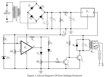
Simple Over Voltage Protector Circuit Diagram

This is the Simple Over Voltage Protector Circuit Diagram. The whole circuit of over voltage protector is build and fabricated around operational amplifier used as comparator. The inverting input is given to pin 2 of op-amp IC (IC1) with reference voltage of 5.1V from zener diode. Similarly, non-inverting input is given to pin no 3 of IC1 use as sensor for over voltage protector for sensing voltage fluctuation in the mains. The two transistors T1 and T2 conduct alternating (i.e. one at a time) according to the voltage of mains.

Simple Over Voltage Protector Circuit Diagram


Simple Over Voltage Protector Circuit Diagram


When voltage is around or below 240V AC transistor T1 is in off-state where T2 energized relay RL1. Similarly, when voltage becomes beyond 240V (i.e. above 240V) T1 is in conducting-stage and T2 is in off-stage which de-energized the relay RL1 and switch-off the appliance.

PARTS LIST

Resistors (all ¼-watt, ~+mn~ 5% Carbon)

R1 = 147 Ω/2W

R2 = 100 Ω/1W

R3 = 330 Ω

R4 = 100 KΩ

R5 = 1.8 KΩ

R6, R7 = 1 KΩ

VR1 = 10 KΩ

VR2 = 22 KΩ
Capacitors

C1, C4, C5 = 0.01 µF

C2 = 1000 µF/25V

C3 = 100 µF/25V
Semiconductors

IC1 = µA741 (Operational Amplifier)

IC2 = 7812

T1= BC547

T2 = SL100

D1, D2, D3, D4, D5 = 1N4007

D6 = 1N4148

ZD1 = 5.1V zener diode
Miscellaneous

X1 = 230V AC primary to 7.5V-0-7.5V, 1A secondary transformer

RL1 = 12V, 200Ω 1 C/O Relay

LED1 = RED

Sourced By:  electronicsproject
Read More

Energy Saving Soldering Station Circuit Diagram

This is the Energy Saving Soldering Station Circuit Diagram. This circuit appears in the test circuit section because the soldering iron is one of the most used service aids. This circuit, will not only save power when the soldering iron in not in use, but will also preserve the tip life.

Energy Saving Soldering Station Circuit Diagram


Energy Saving Soldering Station Circuit Diagram


Circuit Details
a) A 555 timer is configured to delay power on for about minute. During this period the solder iron is connected to AC mains through the "NC" contacts of the relay. The red LED would indicate the initial warm-up of 1 minute after which it goes off and the green LED would light up to indicate that the solder iron is ready to use.

b) IC LM358-A is configured as voltage comparator to check the presence of the solder iron in its stand using a thermistor. The (-)ve input of the comparator is provided with a reference voltage of 6V using R4/R5 potential divider. The (+)ve input is also connected to a potential divider formed with R6 and the thermistor TH1.

If the solder iron is not present in its stand the thermistor would acquire the room temperature. At ambient temperature the resistance of the thermistor would be roughly 10k thus the potential divider R6/TH1 would provide 2.8V at the (+)ve input, which is less than 6V at the (-)ve input. Thus the output of LM358-A remains low and there is no change in the operation; the solder iron continues to get power thru the "NC" contacts of the relay.

c) If the solder iron is present in its stand, the increase in temperature will increase the resistance of the thermistor. As soon as it crosses 33k, the potential divider R6/TH1 provides more than 6V at the (+)ve input hence, the output of LM358-A goes HIGH. This energizes the coil of the relay via NPN transistor T1 and therefore the solder iron is disconnected from the AC mains.

The HIGH output of LM358-A also powers ON the LM358-B network, which is configured as an astable oscillator with a duty cycle of about 20%. The duty cycle is controlled through the potential divider R8/R10. The output is connected to the gate of triac BT136, via opto isolated triac MOC3020. The triac BT136 conducts and switches on the solder iron for 20% of a cycle, thus 80% of power is saved while the solder iron is at rest.


Notes
1) Any value of thermistor may be used but, the value of the R6 should be selected accordingly such that R6/TH1 should provide about 3V at normal temperature. Moreover, the increase in temperature of the spiral steel wire sleeve due to the presence of solder iron should also be taken into account.

2) The triac cannot be replaced with a relay because of two main disadvantages:
a. Continuous rattling sound of the relay contacts could be annoying.
b. The continuous and swift switching of the relay contacts will cause high voltage sparks.

3) The thermistor legs should be covered with heat resistant insulation sleeves and then installed suitably on the iron stand.

4) The 12V power supply (not shown) and the circuit may be enclosed in some suitable box as shown.


Author : Abu-Hafss, Pakistan
Read More

Simple Smart DC fan Circuit Diagram

This is the Simple Smart DC fan Circuit Diagram. In almost all flats the elevators (lifts) are essential. In high rise buildings there are 2 or 3 or even more lifts. These lifts are major source of electrical energy consumption. Why?

The lifts remain idle for most of the time and it is used during peak hours only like in morning from 6 am to 10 am and in evening from 5 pm to 9 pm. So out of 24 hours a lift is used mostly for 8 – 10 hours. Now the problem is, in a lift there is always a fan and a light that stays on continuously. Even if lift is not in used for longer period of time. Although the ON/OFF switches for fan and light are already given, no body turns it OFF. So the fan and light inside the lift stays ON continuously and makes complete waste of electrical energy. Such a waste of valuable electrical energy in this era is not at all desirable. Today all most all the countries are putting their strong efforts to save maximum electrical energy by all means. In India there is heavy scarcity of conventional energy sources from which electricity is produce. So saving electricity and thus these conventional energy sources is must.

  Simple Smart DC fan Circuit Diagram 1
  Simple Smart DC fan Circuit Diagram 1

On this thought an idea came into my mind that why not to add a kind of intelligence in lift fan and light so that it remains ON till there is atleast one person in the lift. And when lift is totally empty fan as well as light automatically turns off. So there should be a kind of sensor in the lift that senses person presence and automatically turns ON or OFF light and fan inside it.

So here i am presenting a simple circuit called smart DC fan that senses any person near by and turns on. when there is no any person it turns off automatically. Later on I have given one more circuit that is with a small change in the same circuit so that it can switch on and off 230 V AC light and fan at a time inside lift.


The circuit is combination of two sub circuits

  • Sensor circuit
  • Monostable multivibrator circuit using IC555

A sensor circuit is built using IR LED, photo diode and two NPN type transistors. IR LED and photo diode are placed nearby on the PCB pointing to same direction in such a way that IR light cannot fall directly on photo diode but only reflected light from any object or person falls on it. Photo diode is connected in reverse bias manner. The output of photo diode is given to 1st transistor Q1 that is connected in switch configuration. Again the output of Q1 is given as input to 2nd transistor Q2 which is again connected in switch configuration. Final output of sensor circuit is taken from output of transistor Q2 that is given to trigger input of IC555. IC555 is configured in monostable multivibrator mode. Resistor R9 and capacitor C3 are timing components of monostable multivibrator. The output of IC555 drives DC motor through Darlington amplifier TIP122. The complete circuit works on 5 V DC supply. DC motor is of also 5 V with 500 RPM.

Circuit operation:

If there is no body is in front of sensor circuit, IR light will not fall on photo diode and its output is high. So transistor Q1 is ON and its output is low. Because this output is applied as input to Q2 its output will be high. So the trigger input of IC555 is high. The IC555 will not get trigger and its output is low. So DC motor fan is off.

When a person (or any object) comes in front of sensor circuit, it reflects IR light that falls on photo diode. So its output goes low. So transistor Q1 input goes low and its output goes high. This makes input of Q2 high and its output low. As Q2 output goes low that applies trigger input to IC555. And its output goes high for the time period set by RC time components. Because this output drives motor, it starts running till the output remains high.

When again a person moves away from sensor photo diode output is high and finally the trigger input to IC555 is also high. So motor continuous to run for the time period given by R9 and C3 (adjustable from 1 to 10 sec) and then it automatically stops.

  Simple Smart DC fan Circuit Diagram 2
   Simple Smart DC fan Circuit Diagram 2

Thus the motor (fan) is ON only if any person is in front of the sensor. If it senses no one in front of it, it turns fan off.

There are few more applications of this circuit also.

The circuit can be used in automatic hand dryer that is used in wash rooms of super markets, multiplexes, hotels or malls. When any one places his/her hand in front of it, the internal motor starts that blows air to dry up hands.

With slight modification this circuit can be used in automatic tap that automatically starts water when a person places his hands below it.

Now let us do a simple modification in the circuit so that it can turn on/off 230 V light and fan simultaneously.

As shown in circuit tab 2, the few changes are

  • In place of darlington amplifier there is simple NPN transistor
  • The transistor drives 5 V 2 C/O (change over) type relay
  • A fan and a bulb both are connected with two common terminals of relay and normally open terminals of relay are given direct 230 V AC supply
  • The second terminal of fan and bulb is given to neutral of AC line

So now when sensor senses a person – it triggers IC555 - transistor becomes ON – it switches ON the relay – bulb and fan both are ON simultaneously.

So using this circuit in a lift, light and fan inside a lift will be ON only while lift is in use. When lift is idle light and fan both will be turned off automatically. SAVE ELECTRICITY – SAVE ENERGY


Author:  A. M. Bhatt
Read More

Simple Electronic Mosquito Repellent Circuit Diagram

This is the Simple Electronic Mosquito Repellent Circuit Diagram. This circuit is very much easy to understand and use. A circuit with minimum components repel mosquito Large number of things like coils, creams, oils is

Simple Electronic Mosquito Repellent Circuit Diagram

Simple Electronic Mosquito Repellent Circuit Diagram


available in the market to repel mosquito. At the same time all these replant is also harmful for the humans too. Oils and creams can led to skin disease, while coils or mats produces toxic fumes which can lead to breathing problem. While in this circuit there is no harm for human being as it produces frequency which human being can not hear. Mosquito repellent generates a frequency ranges from 20-38 KHz. And mosquito runs away from your house as they irritates from these range of frequency.

Human generations are able to hear frequency which has a range from 20Hz to 20 KHz. All the rest frequency above this is considered as a ultrasonic frequency. Many animals and insects are able to hear this range of frequency. Usually in mosquitoes ultra sound is generated by the male ones and female one receives that one. While after breeding female mosquito mainly used to avoid this frequency. And this circuit produces the same frequency as the male one generates, and these creates a stress on the antennae of the mosquito and these keep them away.

Basic principal of this circuit is to connect a such type of buzzer which can produce ultrasonic frequency range. With the help of oscillator in the circuit, buzzer is driven. And in the circuit oscillation is generated by 555 timer which is linked as a astablemultivibrator.

The circuit is connected in the closed mode and thus power is received by the 555 timer. In the starting stage voltage in the capacitor is zero volts. So the voltage at the threshold `as well trigger pin is at zero volts. Now the capacitor starts charging via a resistor R1 and R2.There will be one point when the voltage of capacitor will be higher as compared to threshold voltage. At this stage capacitor starts discharging with the help of resistor R2, which is a discharging pin and it keeps of going downward till it reaches to its original state. Thus the signal at the output pin of IC will be an oscillating signal having 38 KHz frequency. With the help of pin 3 of IC which is out pin of IC 38 KHz frequency drives to 38 KHzpiezo buzzer. This buzzer will produce a ultrasound at a regular interval. By altering the value of resistor R2 we can alter the output frequency.

By changing the value of resistor and capacitor, it can also use as an insect replier as insects are also able to hear ultrasound.

From the source ultrasound are transportable only at 45 degree. So in the situation when there is any hurdles in the track signals get diverted. Also it works on the place where population of mosquito are not much more.

Component Description-

IC (IC1)                     NE555

Capacitor (C1, C2)      0.01uF

Resistor

                R1            760E

                R2            1.5K

PiezoBuzzer(B1)          38KHz

Sourced By:  Kavita Banthiya
Read More

Simple Mains Pulser Circuit Diagram

Mains Pulser Circuit diagram. The pulser is intended to switch the mains voltage on and off at intervals between just under a second and up to 10 minutes. This is useful, for instance, when a mains-operated equipment is to be tested for long periods, or for periodic switching of machinery. Transformer Tr1, the bridge rectifier , and regulator IC1 provide a stable 12V supply rail for IC2 and the relay. The timer is arranged so that the period-determining capacitor can be charged and discharged independently. Four time ranges can be selected by selecting capacitors with the aid of jumpers. Short-circuiting positions 1 and 2 gives the longest time, and short-circuiting none the shortest.

Simple Mains Pulser  Circuit Diagram

Mains Pulser Circuit diagram:
Mains Pulser Circuit Diagram

In the latter case, the 10µF capacitor at pins 2 and 6 of the timer IC determines the time with the relevant resistors. The value of this capacitor may be chosen slightly lower. The two preset potentiometers enable the on and off periods to be set. The 1k resistor in series with one of the presets determines the minimum discharge time. The timer IC switches a relay whose double-pole contacts switch the mains voltage. The LEDs indicate whether the mains voltage is switched through (red) or not (green). The 100mA slow fuse protects the mains transformer and low-voltage circuit. The 4 A medium slow fuse protects the relay against overload.

Read More

Electrical Isolation For I2C Bus Circuit Diagram

This is the simple Electrical Isolation For I2C Bus Circuit Diagram. When the SDA (Serial DAta) lines on both the left and right lines are 1, the circuit is quiescent and optoisolators IC1 and IC2 are not actuated. When the SDA line at the left becomes 0, current flows through the LED in IC1 via R2. The SDA line at the right is then pulled low via D2 and IC1. Optoisolator IC2 does not transfer this 0 to the left, because the polarity of the LED in IC2 is the wrong way around for this level. This arrangement prevents the circuit holding itself in the 0 state for ever. As is seen, the circuit is symmetrical. So, when the SDA line at the right is 0, this is transferred to the left. The lower part of the diagram, intended for the SCL (Serial CLock) line, is identical to the upper part.

Resistors R1, R4, R5, and R8, are the usual 3.3 kΩ pull-up resistors that are obligatory in each I2C line. If these resistors are already present elsewhere in the system, they may be omitted here. The current drawn by the circuit is slightly larger than usual since the pull-up resistors are shunted by the LEDs in the optoisolators and their series resistors. Nevertheless, it remains within the norms laid down in the I2C specification.

Circuit diagram :

Electrical Isolation For I2C Bus Circuit Diagram


Electrical Isolation For I2C Bus Circuit Diagram
Read More

Tri-Waveform Generator Circuit Diagram

This is the simple Tri-Waveform Generator Circuit Diagram. The Tri-Waveform Generator can be used for a number of different uses. The one that I use it for is a signal generator to test circuits. The frequency range is 20 to 20khz. and can be adjusted by R1. The duty cycle or the time that the waveform is high and the time that the waveform is low can be adjusted by R4.

Tri-Waveform Generator Circuit Diagram


Tri-Waveform Generator Circuit Diagram


The purpose of R2 and R3 are to clean up any distortion on the sine wave output. To do this you must hook up the sine wave output to and oscilloscope and adjust R2 & R3 to make the sine wave as accurate as possible.
Read More

Electrification Unit Circuit Diagram

The circuit is intended for carrying out harmless experiments with high-voltage pulses and functions in a similar way as an electrified fence generator. The p.r.f. (pulse repetition frequency) is determined by the time constant of network R1-C3 in the feedback loop of op amp IC1a: with values as specified, it is about 0.5 Hz. The stage following the op amp, IC1b, converts the rectangular signal into narrow pulses. Differentiating network R2-C4, in conjunction with the switching threshold of the Schmitt trigger inputs of IC1b, determines the pulse period, which here is about 1.5 ms. The output of IC1b is linked directly to the gate of thyristor THR1, so that this device is triggered by the pulses.

The requisite high voltage is generated with the aid of a small mains transformer, whose secondary winding is here used as the primary. This winding, in conjunction with C2, forms a resonant circuit. Capacitor C3 is charged to the supply voltage (12 V) via R3.When a pulse output by IC1b triggers the thyristor, the capacitor is discharged via the secondary winding. The energy stored in the capacitor is, however, not lost, but is stored in the magnetic field produced by the transformer when current flows through it. When the capacitor is discharged, the current ceases, whereupon the magnetic field collapses. This induces a counter e.m.f. in the transformer winding which opposes the voltage earlier applied to the transformer.


Simple Electrification Unit Circuit Diagram


Electrification Unit Circuit Diagram


This means that the direction of the current remains the same. However, capacitor C2 is now charged in the opposite sense, so that the potential across it is negative. When the magnetic field of the transformer has returned the stored energy to the capacitor, the direction of the current reverses, and the negatively charged capacitor is discharged via D1 and the secondary winding of the transformer. As soon as the capacitor begins to be discharged, there is no current through the thyristor, which therefore switches off. When C2 is discharged further, diode D1 is reverse-biased, so that the current loop to the transformer is broken, whereupon the capacitor is charged to 12 V again via R3. At the next pulse from IC1b, this process repeats itself.

Since the transformer after each discharge of the capacitor at its primary induces not only a primary, but also a secondary voltage, each triggering of the thyristor causes two closely spaced voltage pulses of opposite polarity. These induced voltages at the secondary, that is, the 230 V, winding, of the transformer are, owing to the higher turns ratio, much higher than those at the primary side and may reach several hundred volts. However, since the energy stored in capacitor C2 is relatively small (the current drain is only about 2 mA), the output voltage cannot harm man or animal. It is sufficient, however, to cause a clearly discernible muscle convulsion.


Author: P. Lay
Copyright: Elektor Electronics
Read More

Cat And Dog Repellent Circuit Diagram

The electronic dog repellent circuit diagram below is a high output ultrasonic transmitter which is primarily intended to act as a dog and cat repeller, which can be used individuals to act as a deterrent against some animals. It should NOT be relied upon as a defence against aggressive dogs but it may help distract them or encourage them to go away and do not consider this as an electronic pest repeller. The ultrasonic dog repellant uses a standard 555 timer IC1 set up as an oscillator using a single RC network to give a 40 kHz square wave with equal mark/space ratio.

This frequency is above the hearing threshold for humans but is known to be irritating frequency for dog and cats. Since the maximum current that a 555 timer can supply is 200mA an amplifier stage was required so a high-power H-bridge network was devised, formed by 4 transistors TR1 to TR4. A second timer IC2 forms a buffer amplifier that feeds one input of the H-bridge driver, with an inverted waveform to that of IC1 output being fed to the opposite input of the H-bridge.

Circuit diagram:
Cat And Dog Repellent Circuit Diagram

This means that conduction occurs through the complementary pairs of TR1/TR4 and TR2/TR3 on alternate marks and spaces, effectively doubling the voltage across the ultrasonic transducer, LS1. This is optimised to generate a high output at ultrasonic frequencies. This configuration was tested by decreasing the frequency of the oscillator to an audible level and replacing the ultrasonic transducer with a loudspeaker; the results were astounding. If the dog repellent circuit was fed by a bench power supply rather than a battery that restrict the available current, the output reached 110dB with 4A running through the speaker which is plenty loud enough!

The Dog and Cat repellant was activated using a normal open switch S1 to control the current consumption, but many forms of automatic switching could be used such as pressure sensitive mats, light beams or PIR sensors. Thus it could be utilise as part of a dog or cat deterrent system to help prevent unwanted damage to gardens or flowerbeds, or a battery powered version can be carried for portable use. Consider also using a lead-acid battery if desired, and a single chip version could be built using the 556 dual timer IC to save space and improve battery life.
Read More

Simple Isolation For PC Boards In Cars Circuit Diagram

Simple Isolation For PC Boards In Cars Circuit Diagram


 These two mounting methods were devised to protect PC boards from vibration when installed in the engine compartment of a car. They could also be used in other applications where vibration is a problem. Method 1 involves rigidly mounting the PC board inside a diecast box and then mounting the box itself to provide vibration isolation. As shown, small grommets are installed in suitably sized holes in the sides of the box.
The box is then secured to angle mounting brackets using M4 screws, washers and nylock nuts. Method 2 involves mounting the diecast case onto the chassis of the car and then mounting the PC board as shown, using M3 screws, grommets, hollow spacers and nylock nuts. In this case, the grommets are fitted into suitably sized holes in the PC board itself. Once the nuts are tightened, the PC board should be able to move slightly, relative to the box. If there is not enough space on the board to fit the grommets, then Method 1 is the way to do it.
Author: David Boyes - Copyright: Silicon Chip Electronics
Read More

Electronic Circuit Simulator Online


The complaint of the majority of users when it comes to electronic circuit simulator is having to download, install and configure the program, which in most cases is a free version of a demonstration and full of limitations. What do you think of using a circuit simulator without having to download or install, and can be used from anywhere provided you have a PC and an Internet connection. This is the online editor of Circuitlab.

Simply enter the site, wait to load the editor and your simulator is ready to use. If you want to save is to create a user on the site through a register. Click here and see this Electronic Circuit Simulator.

 If you liked this article,Take a few Seconds to Share this and leave comments
Read More

Doorbell with Counter Circuit Diagram

This circuit is a doorbell with counter, that means it counts how many times the bell is triggered. It uses a chip synthesizer sound, the HT-2811 ms nothing prevents you from using another device sound generator. The HT-2811 reproduces the sound of a "ding-dong" doorbell. Besides this ic, the circuit includes a CMOS 4026 and Display Driver IC which counts the total number of visitors.

 Electronic Doorbell with Counter Circuit Diagram


Electronic Doorbell with Counter Circuit Diagram
Read More

Soldering Station Weller 40 Watts Circuits Diagram

This is a Soldering Station Weller 40 Watts Circuits Diagram, WLC100 model, she is one of the simplest, however very efficient, ideal for those who want to build a small soldering station. The Weller WLC100 as the main component is a triac which controls the voltage that goes to the resistor, thus making the iron to vary the temperature. He is a very robust Soldering station has a power ranging from 5-40 watts uses the tips (SPG40) and resistance (HE40), ideal for hobbyists, students, and hobbyists. 

Soldering Station Weller 40 Watts Circuits Diagram

Soldering Station Weller 40 Watts Circuits Diagram


List of components 

R1 = 15 Ohms, 1/8 Watt 5%
 P1 = 250K pot
C1 = 823K, 250V
D1, D2 = 1N4004 D3 = Diac, bilateral trigger type Triac
Q1 = 400V/25A, Q4012LPH * (Teccor) or BTA08600c (Philips), or equivalent

ATTENTION: The Triac has an isolated tab, so if you need to replace sure to use the same type.


back
Read More

Dual White Noise and Pink Noise Generator Circuit Diagram

This is a generator circuit which is very useful, it simultaneously generates two types of noise, pink and white. The noise generator is a circuit that produces electrical noise. Noise generators are used to test, measure noise, frequency response, and other parameters. The circuit described here is based on the operational amplifier 741.

 Dual White Noise and Pink Noise Generator Circuit Diagram

Dual White Noise and Pink Noise Generator Circuit Diagram
Read More

Protection Circuit for Input Ports Arduino

This is a Protection for Input Ports Arduino Circuit Diagram. During tests or doing some project, we run the risk of accidentally burn Arduino input. A short circuit protection can prevent a lot of problems and is one less worry, especially against accidents. It is simple, you just need a 1k resistor and a zener diode of 5 Volts, which in the case of commercial zener diode, the voltage is closer to 5.1 V and diode is the 5V1.

 Protection for Input Ports Arduino Circuit Diagram


Read More

Electric Fences Circuit Diagram

This is a Electric Fences Circuit Diagram for rural electrification of about fed with just one 9-volt battery, the circuit is small, so it is portable and handy, its operation is based on NE555 integrated circuit which generates pulses with the same time intervals set by resistor R2 together with P1 default in 100K and C5 which is a 10 uF capacitor, transistor amplifies and sends the transformer 230 volts for 6 volt common.

Electric Fences Circuit Diagram

Electric Fences Circuit Diagram

Read More

4A High-Speed Low-Side Gate Driver Project

This is the simple project of 4A High-Speed Low-Side Gate Driver circuit Diagram. The UCC27518 and UCC27519 single-channel, high-speed, low-side gate driver device is capable of effectively driving MOSFET and IGBT power switches. Using a design that inherently minimizes shoot-through current, UCC27518 and UCC27519 are capable of sourcing and sinking high, peak-current pulses into capacitive loads offering rail-to-rail drive capability and extremely small propagation delay typically 17 ns.

The UCC27518 and UCC27519 provide 4-A source, 4-A sink (symmetrical drive) peak-drive current capability at VDD = 12 V. The UCC27518 and UCC27519 are designed to operate over a wide VDD range of 4.5 V to 18 V and wide temperature range of -40°C to 140°C. Internal Under Voltage Lockout (UVLO) circuitry on VDD pin holds output low outside VDD operating range.

Circuit Project: 4A High-Speed Low-side Gate Driver
Features
  • Low-Cost, Gate-Driver Device Offering Superior Replacement of NPN and PNP Discrete Solutions
  • Pin-to-Pin Compatible With TI’s TPS2828 and the TPS2829
  • 4-A Peak Source and 4-A Peak Sink Symmetrical Drive
  • Fast Propagation Delays (17-ns typical)
  • Fast Rise and Fall Times (8-ns and 7-ns typical)
  • 4.5-V to 18-V Single Supply Range
  • Outputs Held Low During VDD UVLO (ensures glitch free operation at power-up and power-down)
  • CMOS Input Logic Threshold (function of supply voltage with hysteresis)
  • Hysteretic Logic Thresholds for High Noise Immunity
  • EN Pin for Enable Function (allowed to be no connect)
  • Output Held Low when Input Pins are Floating
  • Input Pin Absolute Maximum Voltage Levels Not Restricted by VDD Pin Bias Supply Voltage
  • Operating Temperature Range of -40°C to 140°C
  • 5-Pin DBV Package (SOT-23)
Device Uses
  • Switch-Mode Power Supplies
  • DC-to-DC Converters
  • Companion Gate Driver Devices for Digital Power Controllers
  • Solar Power, Motor Control, UPS
  • Gate Driver for Emerging Wide Band-Gap Power Devices (such as GaN)
Read More

Voltage Monitor Circuit Diagram

This is the project of Voltage Monitor Circuit Diagram. This is a very simple circuit which can be modified to the user's needs. Its operation is simple, when the input voltage is 0, the LED (LO). The LED turns off when the voltage increases to the level determined by R2.


Voltage Monitor Circuit Diagram

Voltage Monitor Circuit Diagram

Read More

Monitor voltage + and - 5VDC + and - 12VDC Circuit Diagram

This circuit is a voltage monitor which operates on fixed testes ± 5 VDC and ± 12 VDC, and is easily constructed as shown in Fig. It is considerably simpler than the normal display using comparators and AND gates. The circuit is not intended to indicate the level of entries. If one of the testes fail, for example, -5 V line fails, the transistor Q3 remains on but the base-emitter junction of T2 is not, so that this transistor is cut off. When this happens, there is no current through D, which then turns off.

Monitor voltage + and - 5VDC + and - 12VDC Circuit Diagram

Monitor voltage + and - 5VDC + and - 12VDC Circuit Diagram

Read More

Generate Electricity from Body Heat Circuit Diagram

The operating principle of this design is unique and extremely simple, the most critical component is the one ba7891 tunnel diode, the circuit that are seven or more soldiers in series and connected to a heat sink large. The sink will serve to accumulate thermal energy, which can be the sun, a fire, the body or any other form of heat energy which is converted into a charge current for NiCd battery.

A tunnel diode is very different from a normal rectifier diode and is characterized by a quick response time, another feature and negative resistance, basically, is explored in this circuit with the purpose of generating electricity from the heat.

 Generate Electricity from Body Heat Circuit Diagram

Generate Electricity from Body Heat Circuit Diagram
Read More