PC Power Saver Circuit Diagram

PC Power Saver Circuit Diagram. This circuit is designed to help minimise the  quiescent power consumption of PCs and  notebooks, using just our old friend the 555  timer and a relay as the main components. The  circuit itself dissipates around 0.5 W in operation (that is, when the connected PC is on);  when switched off (with the relay not energised) the total power draw is precisely zero. A prerequisite for the circuit is a PC or note book with a USB or PS/2 keyboard socket that  is powered only when the PC is on. The power saver can be used to switch PCs  or even whole multi-way extension leads. The unit can be built  into  an  ordinary  mains  adaptor (which must have an earth  pin!) as the photograph of the  author‘s prototype shows. The  PC is plugged in to the socket  at the output of the power saver  unit, and an extra connection  is made to the control input of  the unit from a PS/2 (keyboard or mouse) socket or USB port. Only  the 5 V supply line of the interface is used.
 
PC Power Saver Image  
PC Power Saver Image

When button S1 on the power saver  is pressed the unit turns on, and the  monostable formed by the 555 timer is  triggered via the network composed by  R4 and C7. This drives relay RE1, whose contacts close. The connected PC is now tentatively powered up via the relay for a period  determined  by  P1  (approximately in the range from 5 s to 10 s). If, during this interval, the PC fails to indicate  that it is alive by supplying 5 V from its USB or  PS/2 connector (that is, if you do not switch  it on), the monostable period will expire, the  relay will drop out and any connected device  will be powered down. No further current will  be drawn from the supply, and, of course, it  will not be possible to turn the PC on. When-ever you want to turn the PC on, you must  always press the button on the power saver  shortly beforehand. 

If, however, 5 V is delivered by the PC to the  input of optocoupler IC2 before the monostable times out (which will be the case if the  PC is switched on during that period), the  transistor in the optocoupler will conduct  and discharge capacitor C6. The monostable  will now remain triggered and the relay will  remain energised until the PC is switched off  and power disappears from its USB or PS/2  interface. Then, after the monostable time  period expires, the relay will drop out and the  power saver will disconnect itself from the mains. There is no need to switch anything  else off: just shut down the system and the  power saver will take care of the rest.
 
Circuit diagram :
PC Power Saver-Circuit-Diagram
PC Power Saver Circuit Diagram
 
It is also  possible to leave the machine as it updates its  software, and the power saver will do its job  shortly after the machine shuts down. Power for the unit itself is obtained using a  simple supply circuit based around a miniature transformer. Alternatively, a 12 V mains  adaptor can be used, as long as a relay with a  12 V coil voltage is used for RE1. In his proto-type the author used a relay with a 24 V coil  connected as shown directly to the positive  side of reservoir capacitor C2, the 555 being  powered from 12 V regulated from that sup-ply using R1 and D1. A fixed resistor can of  course be used in place of P1 if desired. If the  adjustment range of P1 is not sufficient (for  example if the PC powers up very slowly) the  monostable period can be increased by using  a larger capacitor at C6.  The relay must have at least two normally-open (or changeover) contacts rated at at  least 8 A. The contact in parallel with S1 is used to supply power to the device  itself, and the other contact carries  all the current for the connected  PC  or  for  the  ex tension  lead  to  which  the  PC  and  peripherals  are  connected. 

Pushbutton S1 must be rated for 230 VAC  (US: 120 VAC) operation: this is no place to  make economies. The coil current for the relay  flows through LED D5, which must therefore  be a 20 mA type. If a low-current LED is used,  a 120 Ω resistor can be connected in parallel with it to carry the remaining current.  The Fujitsu FTR-F1CL024R relay used in the  author’s prototype has a rated coil current of  16.7 mA. Optocoupler IC2 provides isolation between  the circuit and the PC, and is protected from  reverse polarity connection by diode D4. The power saver should be built into an insulated enclosure and great care should be  taken to ensure that there is proper isolation  between components and wires carrying the  mains voltage and the other parts of the circuit. In particular, the connection to the PC  and associated components (R6, C5, D4 and  IC2) should be carefully arranged with at least  a 6 mm gap between them and any part of  the circuit at mains potential.


Author : Wolfgang Gscheidle (Germany) - Copyright : Elektor
Read More

USB-Powered PIC Programmer Circuit Diagram

This simple circuit can be used to program the PIC16F84 and similar "flash memory" type parts. It uses a cheap 555 timer IC to generate the programming voltage from a +5V rail, allowing the circuit to be powered from a computer’s USB port. The 555 timer (IC1) is configured as a free-running oscillator, with a frequency of about 6.5kHz. The output of the timer drives four 100nF capacitors and 1N4148 diodes wir-ed in a Cockroft-Walton voltage multiplier configuration.

USB-Powered PIC Programmer Circuit diagram:

usb-powered-pic-programmer-circuit-diagramw
USB-Powered PIC Programmer Circuit Diagram

The output of the multiplier is switched through to the MCLR/Vpp pin of the PIC during programming via a 4N28 optocoupler. Diodes ZD1 and D5 between the MCLR/Vpp pin and ground clamp the output of the multiplier to about 13.6V, ensuring that the maximum input voltage (Vihh) of the PIC is not exceeded. A 100kΩ resistor pulls the pin down to a valid logic low level (Vil) when the optocoupler is not conducting. The circuit is compatible with the popular "JDM" programmer, so can be used with supporting software such as "ICProg" (see http://www.ic-prog.com).


Author: Luke Weston - Copyright: Silicon Chip Electronics
Read More

Intelligent Presence Simulator Circuit project

Intelligent Presence Simulator Circuit diagram. However effective a domestic alarm system may be, it’s invariably better if it never goes off, and the best way to ensure this is to make potential burglars think the premises are occupied. Indeed, unless you own old masters or objects of great value likely to attract ‘professional’ burglars, it has to be acknowledged that the majority of burglaries are committed by ‘petty’ thieves who are going to be looking more than anything else for simplicity and will prefer to break into homes whose occupants are away.

Rather than simply not going on holiday – which is also one solution to the problem (!) – we’re going to suggest building this intelligent presence simulator which ought to put potential burglars off, even if your home is subjected to close scrutiny. Like all its counterparts, the proposed circuit turns one or more lights on and off when the ambient light falls, but while many devices are content to generate fixed timings, this one works using randomly variable durations.

Intelligent Presence Simulator Circuit diagram:

Intelligent Presence Simulator Circuit diagram
Intelligent Presence Simulator Circuit Diagram

So while other devices are very soon caught out simply by daily observation (often from a car) because of their too-perfect regularity, this one is much more credible due to the fact that its operating times are irregular. The circuit is very simple, as we have employed a microcontroller – a ‘little’ 12C508 from Microchip, which is more than adequate for such an application. It is mains powered and uses rudimentary voltage regulation by a zener diode.


A relay is used to control the light(s); though this is less elegant than a triac solution, it does avoid any interference from the mains reaching the microcontroller, for example, during thunderstorms. We mustn’t forget this project needs to work very reliably during our absence, whatever happens. The ambient light level is measured by a conventional LDR (light dependent resistor), and the lighting switching threshold is adjustable via P1 to suit the characteristics and positioning of the LDR.

Note that input GP4 of the PIC12C508 is not analogue, but its logic switching threshold is very suitable for this kind of use. The LED connected to GP1 indicates the circuit’s operating mode, selected by grounding or not of GP2 or GP3 via override switch S1. So there are three possible states: permanently off, permanently on, and automatic mode, which is the one normally used. Given the software programmed into the 12C508 (‘firmware’) and the need to generate very long delays so as to arrive at lighting times or an hour or more, it has been necessary to make the MCU operate at a vastly reduced clock frequency.

PCB Layout:
pcb-layout-of-intelligent-presence-sim
PCB Layout Of Intelligent Presence Simulator

In that case, a crystal-controlled clock is no longer suitable, so the R-C network R5/C3 is used instead. For sure, such a clock source is less stable than a crystal, but then in an application like this, that may well be what we’re after as a degree of randomness is a design target instead of a disadvantage. Our suggested PCB shown here takes all the components for this project except of course for S1, S2, and the LDR, which will need to be positioned on the front panel of the case in order to sense the ambient light intensity.

The PCB has been designed for a Finder relay capable of switching 10 A, which ought to prove adequate for lighting your home, unless you live in a replica of the Palace of Versailles. The program to be loaded into the 12C508 is available for free download from the Elektor website as file number 080231-11.zip or from the author’s own website: www.tavernier-c.com. On completion of the solder work the circuit should work immediately and can be checked by switching to manual mode.

The relay should be released in the ‘off’ position and energized in the ‘on’ position. Then all that remains is to adjust the day/night threshold by adjusting potentiometer P1. To do this, you can either use a lot of patience, or else use a voltmeter – digital or analogue, but the latter will need to be electronic so as to be high impedance – connected between GP4 and ground. When the light level below which you want the lighting to be allowed to come on is reached, adjust P1 to read approximately 1.4 V on the voltmeter.

If this value cannot be achieved, owing to the characteristics of your LDR, reduce or increase R8 if necessary to achieve it (LDRs are known to have rather wide production tolerances). Equipped with this inexpensive accessory, your home of course hasn’t become an impregnable fortress, but at least it ought to appear less attractive to burglars than houses that are plunged into darkness for long periods of time, especially in the middle of summer. (www.tavernier-c.com)

COMPONENTS LIST Resistors
R1 = 1k 500mW
R2 = 4k7
R3 = 560R
R4,R6 = 10k
R5 = 7k5
R 7 = LDR
R8 = 470k to 1 M
P1 = 470k potentiometer
Capacitors
C1 = 470µF 25V
C2 = 10µF 25V
C3 = 1nF5
C4 = 10nF
Semiconductors
D1,D2 = 1N4004
D3 = diode zener 4V7 400 mW
LED1 = LED, red
D4 = 1N4148
T1 = BC547
IC1 = PIC12C508, programmed, see Downloads
Miscellaneous
RE1 = relay, 10A contact
S1 = 1-pole 3-way rotary switch
F1 = fuse 100 mA
TR1 = Mains transformer 2x9 V, 1.2 -3 VA
4 PCB terminal blocks, 5 mm lead pitch
5 solder pins 
Read More

Simple DCF77 Preamplifier Circuit Diagram

Simple DCF77 Preamplifier Circuit Diagram. A popular project among microcontroller aficionados is to build a radio-controlled clock. Tiny receiver boards are available, with a pre-adjusted ferrite antenna, that receive and demodulate the DCF77 time signal broadcast from Mainf lingen in Germany. DCF77 has a range of about 1,000 miles. All the microcontroller need do is decode the signal and output the results on a display. The reception quality achieved by these ready-made boards tends to be proportional to their price.

In areas of marginal reception a higher quality receiver is needed, and a small selective preamplifier stage will usually improve the situation further. The original ferrite antenna is desoldered from the receiver module and connected to the input of the preamplifier. This input consists of a source follower (T1) which has very little damping effect on the resonant circuit. A bipolar transistor (T2) provides a gain of around 5 dB. The output signal is coupled to the antenna input of the DCF77 module via a transformer.

The secondary of the transformer, in conjunction with capacitors C4 and C5, forms a resonant circuit which must be adjusted so that it is centered on the carrier frequency. An oscilloscope is needed for this adjustment, and a signal generator, set to generate a 77.5 kHz sine wave, is also very useful. This signal is fed, at an amplitude of a few milli-volts, into the antenna input. With the oscilloscope connected across C4 and C5 to monitor the signal on the output resonant circuit, trimmer C5 is adjusted until maximum amplitude is observed.

DSf 77-preamplifier-circuit-diagram DCF77 Preamplifier Circuit Diagram

DCF77 Breadboard circuit


It is essential that the transformer used is suitable for constructing a resonant circuit at the carrier frequency. Our proto-type used a FT50-77 core from Amidon on which we made two 57-turn windings. It is also possible to trim the resonant frequency of the circuit by using a transformer whose core can be adjusted in and out. In this case, of course, the trimmer capacitor can be dispensed with.
Read More

Multitasking Pins Circuit Diagram

Multitasking Pins Circuit Diagram It’s entirely logical that low-cost miniature microcontrollers have fewer ‘legs’ than their bigger brothers and sisters – sometimes too few. The author has given some consideration to how to economise on pins, making them do the work of several. It occurred that one could exploit the high impedance feature of a tri-state output. In this way the signal produced by the high impedance state could be used for example as a CS signal of two ICs or else as a RD/ WR signal.

All we need are two op-amps or comparators sharing a single operating voltage of 5 V and outputs capable of reaching full Low and High levels in 5-V operation (preferably types with rail-to-rail outputs). Suitable examples to use are the LM393 or LM311.The resistances in the voltage dividers in this circuit are uniformly 10 kilo ohms. Consequently input A lies at half the operating voltage (2.5 V), assuming nothing is connected to the input – or the microcontroller pin connected is at high impedance. 


multitasking pins circuit diagram Multitasking Pins Circuit Diagram


The non-inverting input of IC1A lies at two thirds and the inverting input of IC1B at one third of the operating voltage, so that in both cases the outputs are set at High state. If the microcontroller pin at input A becomes Low, the output of IC1B becomes Low and that of IC1A goes High. If A is High, everything is reversed.
Read More

Universal PIC Programmer Circuit Diagram

This simple programmer will accept any device that's supported by software (eg, IC-Prog 1.05 by Bonny Gijzen at www.ic-prog.com). The circuit is based in part on the ISP header described in the SILICON CHIP "PIC Testbed" project but also features an external programming voltage supply for laptops and for other situations where the voltage present on the RS232 port is insufficient. This is done using 3-terminal regulators REG1 & REG2. The PIC to be programmed can be mounted on a protoboard. This makes complex socket wiring to support multiple devices unnecessary. 16F84A, 12C509, 16C765 and other devices have all been used successfully with this device.

Circuit diagram:


Simple Universal PIC Programmer Circuit Diagram


Read More

Contrast Control Circuit Diagram for LCDs

This is a simple project of Contrast Control Circuit Diagram for LCDs. The adjustment control for the contrast of an LC-Display is typically a 10-k potentiometer. This works fine, provided that the power supply voltage is constant. If this is not the case (for example, with a battery power supply) then the potentiometer has to be repeatedly adjusted. Very awkward, in other words. The circuit described here offers a solution for this problem. 

The aforementioned potentiometer is intended to maintain a constant current from the contrast connection (usually pin 3 or Vo) to ground. A popular green display with 2x16 characters ‘supplies’ about 200 µA. At a power supply voltage of 5 V there is also an additional current of 500 µA in the potentiometer itself. Not very energy efficient either. Now there is an IC, the LM334, which, with the aid of one resistor, can be made into a constant current source. The circuit presented here ensures that there is a current of 200 µA to ground, independent of the power supply voltage. By substituting a 2.2-k? potentiometer for R1, the current can be adjusted as desired.

Circuit diagram:The value of R1 can be calculated as follows: R1 = 227x10-6 x T / I. Where T is the temperature in Kelvin and I is the current in ampères. In our case this results in:
R1 = 227x10-6 x 293 /
(200x10-6)
R1 = 333R

Note that the current supplied by the LM334 depends on the temperature. This is also true for the current from the display, but it is not strictly necessary to have a linear relationship between these two. Temperature variations of up to 10° will not be a problem however. This circuit results in a power saving of over 25% with an LCD that itself draws a current of 1.2 mA. In a battery powered application this is definitely worth the effort! In addition, the contrast does not need to be adjusted as the battery voltage reduces. When used with LCDs with new technologies such as OLED and PLED it is advisable to carefully test the circuit first to determine if it can be used to adjust the brightness.

Contrast Controller Circuit Diagram For LCDs:

Contrast Controller Circuit Diagram For LCDs

The value of R1 can be calculated as follows: R1 = 227x10-6 x T / I. Where T is the temperature in Kelvin and I is the current in ampères. In our case this results in:
  • R1 = 227x10-6 x 293 /
  • (200x10-6)
  • R1 = 333R
Note:
  • The current supplied by the LM334 depends on the temperature. This is also true for the current from the display, but it is not strictly necessary to have a linear relationship between these two. Temperature variations of up to 10° will not be a problem however. This circuit results in a power saving of over 25% with an LCD that itself draws a current of 1.2 mA. In a battery powered application this is definitely worth the effort! In addition, the contrast does not need to be adjusted as the battery voltage reduces. When used with LCDs with new technologies such as OLED and PLED it is advisable to carefully test the circuit first to determine if it can be used to adjust the brightness.
Read More

The Gentle Touch Circuit Diagram

This is a project of Gentle Touch Circuit Diagram. Consumer appliances these days hardly ever have a proper mains switch. Instead, appliances are turned on and off at the touch of a button on the remote control, just like any other function. This circuit shows how a device (as long as it does not draw too high a current) can be switched on and off using a push button. The approach requires that a micro controller is already available in the circuit, and a spare input port pin and a spare output port pin are required, along with a little software. When power is applied T1 initially remains turned off. When the button is pressed the gate of T1 is taken to ground and the p-channel power MOSFET conducts. The micro controller circuit is now supplied with power. Within a short period the micro controller must take output PB1 high. This turns on n-channel MOSFET T1 which in turn keeps T1 turned on after the push-button is released.

Now the micro controller must poll the state of the push-button on its input port (PB0) at regular intervals. Immediately after switch-on it will detect that the button is pressed (a low level on the input port pin), and it must wait for the button to be released. When the button is next pressed the device must switch itself of f: to do this the firmware running in the micro controller must set the output port pin to a low level. When the button is subsequently released T1 will now turn off and the supply voltage will be removed from the circuit.

The circuit itself draws no current in the off state, and for (rechargeable) battery-powered appliances it is therefore best to put the switch before the voltage regulator. For mains-powered devices the switch can also be fitted before the voltage regulator (after the rectifier and smoothing capacitor). Since there is no mains switch there will still be a small standby current draw in this case due to the transformer. Be careful not to exceed the maximum gate-source voltage specification for T1: the IRFD9024 device suggested can withstand up to 20 V. At lower voltages R2 can be replaced by a wire link; otherwise suitable values for the voltage divider formed by R1 and R2 must be selected.

The Gentle Touch Circuit Diagram

 The Gentle Touch Circuit Diagram

The author has set up a small website for this project at http://reweb.fh-weingarten.de/elektor, which gives source code examples (which include dealing with push button contact bounce) for AVR micro controllers suitable for use with AVR Studio and GNU C. Downloads are also available at http://www.elektor.com.
Read More

Simple PIC Controlled Relay Driver Circuit Diagram

This is a simple project of PIC Controlled Relay Driver circuit is a relay driver that is based on a PIC16F84A microcontroller. The board includes four relays so this lets us to control four distinct electrical devices. The controlled device may be a heater, a lamp, a computer or a motor. To use this board in the industrial area, the supply part is designed more attentively. To minimize the effects of the ac line noises, a 1:1 line filter transformer is used.

PIC-Controlled-Relay Driver Final

The transformer is a 220V to 12V, 50Hz and 3.6VA PCB type transformer. The model seen in the photo is HRDiemen E3814056. Since it is encapsulated, the transformer is isolated from the external effects. A 250V 400mA glass fuse is used to protect the circuit from damage due to excessive current. A high power device which is connected to the same line may form unwanted high amplitude signals while turning on and off. To bypass this signal effects, a variable resistor (varistor) which has a 20mm diameter is paralelly connected to the input.

Simple PIC Controlled Relay Driver Circuit Diagram

 
 Controller-Schematic Circuit

Another protective component on the AC line is the line filter. It minimizes the noise of the line too. The connection type determines the common or differential mode filtering. The last components in the filtering part are the unpolarized 100nF 630V capacitors. When the frequency increases, the capacitive reactance (Xc) of the capacitor decreases so it has a important role in reducing the high frequency noise effects. To increase the performance, one is connected to the input and the other one is connected to the output of the filtering part.

Supply-Schematic circuit

After the filtering part, a 1A bridge diode is connected to make a full wave rectification. A 2200 uF capacitor then stabilizes the rectified signal. The PIC controller schematic is given in the project file. It contains PIC16F84A microcontroller, NPN transistors, and SPDT type relays. When a relay is energised, it draws about 40mA. As it is seen on the schematic, the relays are connected to the RB0-RB3 pins of the PIC via BC141 transistors. When the transistor gets cut off, a reverse EMF may occur and the transistor may be defected. To overcome this unwanted situation, 1N4007 diodes are connected between the supply and the transistor collectors. There are a few number of resistors in the circuit. They are all radially mounted. Example C and HEX code files are included in the project file. It energizes the next relay after every five seconds.

The components are listed below.
1 x PIC16F84A Microcontroller
1 x 220V/12V 3.6VA (or 3.2VA) PCB Type Transformer (EI 38/13.6)
1 x Line Filter (2x10mH 1:1 Transformer)
4 x 12V Relay (SPDT Type)
4 x BC141 NPN Transistor
5 x 2 Terminal PCB Terminal Block
4 x 1N4007 Diode
1 x 250V Varistor (20mm Diameter)
1 x PCB Fuse Holder
1 x 400mA Fuse
2 x 100nF/630V Unpolarized Capacitor
1 x 220uF/25V Electrolytic Capacitor
1 x 47uF/16V Electrolytic Capacitor
1 x 10uF/16V Electrolytic Capacitor
2 x 330nF/63V Unpolarized Capacitor
1 x 100nF/63V Unpolarized Capacitor
1 x 4MHz Crystal Oscillator
2 x 22pF Capacitor
1 x 18 Pin 2 Way IC Socket
4 x 820 Ohm 1/4W Resistor
1 x 1K 1/4W Resistor
1 x 4.7K 1/4W Resistor
1 x 7805 Voltage Regulator (TO220)
1 x 7812 Voltage Regulator (TO220)
1 x 1A Bridge Diode


Read More

Simple AVR Dongle Circuit Diagram

AVR Dongle Circuit diagram. This circuit is intended to program AVR controllers such as the AT90S1200 via the parallel port. The circuit is extremely simple. IC1 provides buffering for the signals that travel from the parallel port to the microcontroller and vice versa. This is essentially everything that can be said about the circuit. The two boxheaders (K2 and K3) have the ‘standard’ ISP (in system programming) pinout for the AVR controllers. The manufacturer recommends these two pinouts in an attempt to create a kind of standard for the in-circuit programming of AVR-controllers. These connections can be found on many development boards for these controllers. The software carries out the actual programming task.

AVR Dongle Circuit diagram :

AVR_Dongle_Circuit_Diagramw
AVR Dongle Circuit Diagram

It is therefore necessary to have a program (ATMEL AVR ISP), which is available as a free download from http://www.atmel.com. The construction of the circuit will have to made on standard prototype board, since we didn’t design a PCB for this circuit. This should not present any difficulties considering the small number of parts involved. We recommend that inexperienced builders first make a copy of the circuit and cross off each connection on the schematic once it has been made on the board. This makes it easy to check afterwards whether all connections have been made or not.
Read More

Audible Logic Probe Circuit Diagram

When testing circuits with a logic probe, it is sometimes difficult to watch the LEDS on the probe to determine the logic state. With this probe the logic states are audible. This probe is designed for TTL circuits only but could be modified for CMOS. The way it works is as follows. The 5 volt power source will be the circuit under test. Clip the ground input of the probe to the ground of the circuit being tested. The other input lead is used to probe the different chips of the circuit being tested. Any input greater then 2 volts will be high and output a high tone through the speaker. Any input less then .8 volts will be low and produce a low tone through the speaker.

Audible Logic Probe Circuit Diagram


Audible Logic Probe circuit diagram


Source : extreamcircuits.net
Read More

Multitasking Pins Circuit Diagram

It’s entirely logical that low-cost miniature micro controllers have fewer ‘legs’ than their bigger brothers and sisters – some-times too few. The author has given some consideration to how to economies on pins, making them do the work of several. It occurred that one could exploit the high-impedance feature of a tri-state output. In this way the signal produced by the high-impedance state could be used for example as a CS signal of two ICs or else as a RD/WR signal. All we need are two op-amps or comparators sharing a single operating voltage of 5 V and outputs capable of reaching full Low and High levels in 5-V operation (preferably types with rail-to-rail outputs).

Multitasking Pins Circuit diagram:

Multitasking Pins Circuit Diagram

Suitable examples to use are the LM393 or LM311. The resistances in the voltage dividers in this circuit are uniformly 10k. Consequently input A lies at half the operating voltage (2.5V), assuming nothing is connected to the input - or the micro controller pin connected is at high impedance. The non-inverting input of IC1A lies at two-thirds and the inverting input of IC1B at one third of the operating voltage, so that in both cases the outputs are set at High state. If the micro controller pin at input A becomes Low, the output of IC1B becomes Low and that of IC1A goes High. If A is High, everything is reversed.
Read More

zBot :10-A Power Stage for DC Motor Circuit Diagram

zBot :10-A Power Stage for DC Motor Circuit Diagram . If you look at the chassis of the zBot vehicle1, you’ll find two parts requiring intelligent control: the steering servo and the DC motor. The so called H-bridge is the normal circuit for electronic control of revolution speed and direction. The DC motor of a Tamiya car is powerful enough to propel zBot at up to 20 miles per hour.
.
The motor then consumes more than 10 A, so we choose high-current power MOSFETs for the driver stage. There are lots of different devices to choose from. The MOSFET we require has to supply the maximum motor current and, importantly, it has to be switched with gate voltages of about 5 V. In this case, the microcontroller switches the power stage (‘low side’) directly. For high side driving level shifters are necessary. The schematic of the H-bridge power stage shows a few inverters, NAND gates and two tri-stateable drivers. These logic functions are very important as the easier way, i.e.., directly controlling all four MOSFET has a fatal disadvantage.

zBot :10-A Power Stage for DC Motor Circuit Diagram


zBot :10-A Power Stage for DC Motor Circuit Diagram


In case of a software crash it could happen that two ore more MOSFETs are switched on incor-rectly for exam-ple, T4 and T7. In that case, the current through the transistors is limited by the internal resistors of the MOSFETs (about 10 mO) only. Such a fatal error would destroy the MOSFETs. The logic functions configured here effectively avoid illegal states.To control the DC motor, three signals are needed: DIR, PWM and STOP. DIR controls the direction of the motor revolution, PWM the speed, and STOP brakes the motor.

The software module for the DC motor is called dcm.c.(070172-I) The complete document called Zbot  the Robot Experimental Platform is available for free downloading from the Elektor Electronics website. The file number is 070172-11.zip (July/August 2007).

Sourced by : Circuitsstream.blogspot.com
Read More

Simple 12 V Bidirectional Motor Control Circuit Diagram

12 V Bidirectional Motor Control Circuit Diagram diagram. This simple circuit drives DC motors with a maximum current of 1 A and can be built with readily available components.The output voltage is adjustable between 0 and 14 V and the polarity can be changed so that not only motor speed but also rotation direction can be adjusted by turning a knob. 

The circuit is also ideal as a controller for a DC model railway or small low voltage hobby tool. Power for the circuit is supplied by a 18 V mains transformer rated at 1.5 A. Diodes D1to D4 rectify the supply and capacitor C1 provides smoothing to give a DC output voltage of around 24 V. A classic ‘H’ bridge configuration is made up with transistors T1/T3 and T2/T4. Transistors T5 and T6 together with resistors R7 and R8 provide the current sense and limiting mechanism. The maximum output current limit can be changed from 1 A by using different value resistors for R7 and R8: IOUT = 0.6 V / R where R gives the value for R7 and R8. For increased current limit the mains transformer and diodes will need to be changed to cope with the extra current as well as the four transistors used in the bridge configuration. 


12 V Bidirectional Motor Control Circuit Diagram diagram:


12 V Bidirectional Motor Control Circuit
 
  12 V Bidirectional Motor Control Circuit Diagram
 
Motor speed control and direction is controlled by a twin-ganged linear pot (P1). The two tracks of P1 together with R1/R2 and R3/R4 form two adjustable potential divider networks. Wiring to the track ends are reversed so that as the pot is turned the output voltage of one potential divider increases while the other decreases and vice versa. 

In the midway position both dividers are at the same voltage so there is no potential difference and the motor is stationary. As the pot is rotated the potential difference across the motor increases and it runs faster. The voltage drop across D5 and D6 is equal to the forward voltage drop VBE of the bridge transistors and ensures that the motor does not oscillate in the off position with the pot at its mid point.
Read More

Project of DCF77 Preamplifier Circuit Diagram

Project of DCF77 Preamplifier Circuit Diagram . A popular project among micro controller aficionados is to build a radio-controlled clock. Tiny receiver boards are available, with a pre-adjusted ferrite antenna, that receive and demodulate the DCF77 time signal broadcast from Mainf lingen in Germany. DCF77 has a range of about 1,000 miles. All the micro controller need do is decode the signal and output the results on a display. The reception quality achieved by these ready-made boards tends to be proportional to their price.

In areas of marginal reception a higher quality receiver is needed, and a small selective preamplifier stage will usually improve the situation further.

The original ferrite antenna is desoldered from the receiver module and connected to the input of the preamplifier. This input consists of a source follower (T1) which has very little damping effect on the resonant circuit. A bipolar transistor (T2) provides a gain of around 5 dB. The output signal is coupled to the antenna input of the DCF77 module via a transformer.

DCF77 Preamplifier Circuit Diagram

The secondary of the transformer, in conjunction with capacitors C4 and C5, forms a resonant circuit which must be adjusted so that it is centered on the carrier frequency. An oscilloscope is needed for this adjustment, and a signal generator, set to generate a 77.5 kHz sine wave, is also very useful. This signal is fed, at an amplitude of a few milli-volts, into the antenna input. With the oscilloscope connected across C4 and C5 to monitor the signal on the output resonant circuit, trimmer C5 is adjusted until maximum amplitude is observed.

It is essential that the transformer used is suitable for constructing a resonant circuit at the carrier frequency. Our proto-type used a FT50-77 core from Amidon on which we made two 57-turn windings. It is also possible to trim the resonant frequency of the circuit by using a transformer whose core can be adjusted in and out. In this case, of course, the trimmer capacitor can be dispensed with.


Sourced by: Streampowers
Read More

Project of LCD Module in 4-bit Mode Circuit

LCD Module in 4-bit Mode Circuit diagram. In many projects use is made of alphanumeric LCDs that are driven internally by Hitachi’s industry-standard HD44780 controller. These displays can be driven either in 4-bit or 8-bit mode. In the first case only the high nibble (D4 to D7) of the display’s data bus is used. The four unused connections still deserve some closer attention. The data lines can be used as either inputs or outputs for the display. It is well known that an unloaded output is fine, but that a floating high-impedance input can cause problems. So what should you do with the four unused data lines when the display is used in 4-bit mode? This question arose when a circuit was submitted to us where D0-D3 where tied directly to GND (the same applies if it was to +5 V) to stop the problem of floating inputs.

The LCD module was driven directly by a microcontroller, which was on a development board for testing various programs and I/O functions. There was a switch present for turning off the enable of the display when it wasn’t being used, but this could be forgotten during some experiments. When the R/Wline of the display is permanently tied to GND (data only goes from the microcontroller to the display) then the remaining lines can safely be connected to the supply (+ve or GND). In this application however, the R/Wline was also controlled by the microcontroller. When the display is initialised correctly then nothing much should go wrong. The data sheet for the HD44780 is not very clear as to what happens with the low nibble during initialisation.

LCD Module in 4-bit Mode Circuit diagram :

LCD module_in_4-bit_Mode_Circuit_Diagramw
LCD Module in 4-bit Mode Circuit Diagram

After the power-on reset the display will always be in 8-bit mode. A simple experiment (see the accompanying circuit) reveals that it is safer to use pull-down resistors to GND for the four low data lines. The data lines of the display are configured as outputs in this circuit (R/Wis high) and the ‘enable’ is toggled (which can still happen, even though it is not the intention to communicate with the display). Note that in practice the RS line will also be driven by an I/O pin, and in our circuit the R/W line as well. All data lines become high and it’s not certain if (and if so, for how long) the display can survive with four shorted data lines. The moral of the story is: in 4-bit mode you should always tie D0-D3 via resistors to ground or positive.
Read More

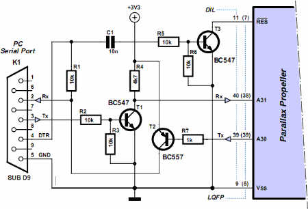
Programming The Propeller IC Circuit Diagram

Programming The Propeller IC Circuit diagram. Parallax, well known for its successful Basic Stamp IC, has recently introduced the Propeller: a new microcontroller with a certain difference. It packs no less than eight 32-bit processors (referred to as COGs in Propeller jargon) into a single package with only 40 pins. That design takes genuine simultaneous multiprocessing possible, and the sophisticated internal structure of the device makes it relatively easy to implement video and signal-processing applications. The Propeller can be programmed in assembly language or the high-level Spin language. The processor and the programming tools were developed entirely in-house by Parallax, with the hardware being designed from scratch starting at the transistor level.

Programming The Propeller IC Circuit diagram:


Programming The Propeller IC Circuit diagram


The basic idea behind that was to avoid becoming involved in all sorts of patent disputes with other manufacturers. The result is astounding, and for software developers it certainly requires a change in mental gears. As is customary with modern microprocessors, the Propeller has a simple serial programming interface. The developer’s toolkit from Parallax has a modern USB port for that purpose, but a reasonably simple alternative (illustrated here) is also possible for anyone who prefers to work with the familiar RS232 port. Don’t forget that the Propeller works with a 3.3-V supply voltage.
Read More